SLVSEW8B August 2019 – December 2019 TPS66020 , TPS66021
PRODUCTION DATA.
- 1 Features
- 2 Applications
- 3 Description
- 4 Revision History
- 5 Pin Configuration and Functions
-
6 Specifications
- 6.1 Absolute Maximum Ratings
- 6.2 ESD Ratings
- 6.3 Recommended Operating Conditions
- 6.4 Recommended Supply Load Capacitance
- 6.5 Thermal Information
- 6.6 PP5V Power Switch Characteristics
- 6.7 PPHV Power Switch Characteristics
- 6.8 Power Path Supervisory
- 6.9 VBUS LDO Characteristics
- 6.10 Thermal Shutdown Characteristics
- 6.11 Input-output (I/O) Characteristics
- 6.12 Power Consumption Characteristics
- 6.13 Typical Characteristics
- 7 Parameter Measurement Information
-
8 Detailed Description
- 8.1 Overview
- 8.2 Functional Block Diagram
- 8.3 Feature Description
- 8.4 Device Functional Modes
-
9 Application and Implementation
- 9.1 Application Information
- 9.2
Typical Application
- 9.2.1 Design Requirements
- 9.2.2
Detailed Design Procedure
- 9.2.2.1 External Current Reference Resistor (RIREF)
- 9.2.2.2 External VLDO Capacitor (CVLDO)
- 9.2.2.3 PP5V Power Path Capacitance
- 9.2.2.4 PPHV, VBUS Power Path Capacitance
- 9.2.2.5 VBUS TVS Protection (Optional)
- 9.2.2.6 VBUS Schottky Diode Protection (Optional)
- 9.2.2.7 VBUS Overvoltage Protection (Optional)
- 9.2.2.8 Dead Battery Support
- 9.2.2.9 Fast Role Swap (FRS) (Optional)
- 9.2.3 Application Curves
- 10Power Supply Recommendations
- 11Layout
- 12Device and Documentation Support
- 13Mechanical, Packaging, and Orderable Information
Package Options
Mechanical Data (Package|Pins)
- YBG|28
Thermal pad, mechanical data (Package|Pins)
Orderable Information
9.2 Typical Application
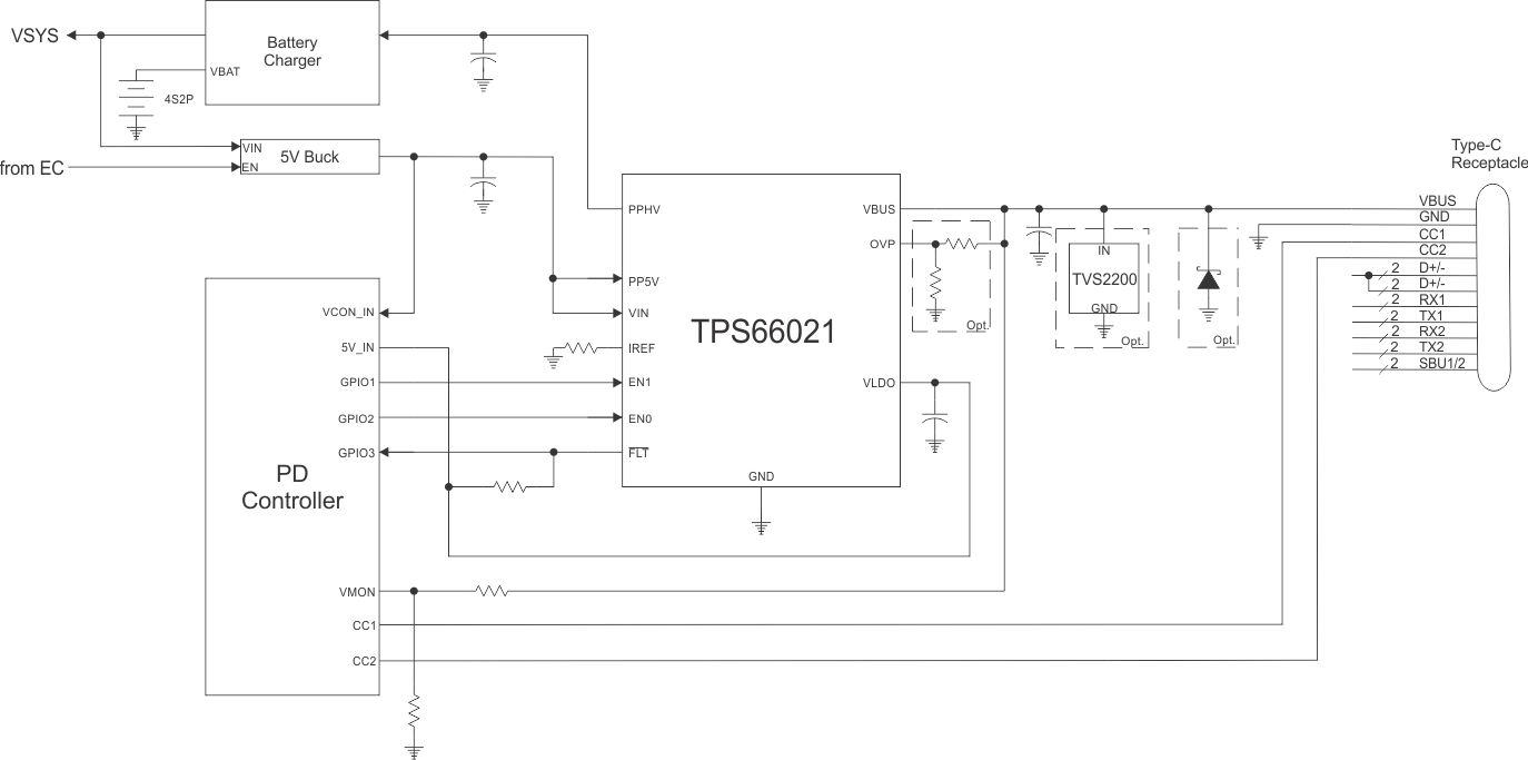
Figure 28 shows a USB Type-C single port design using a Power Delivery (PD) controller that supports 5-V operation. For this system, a single 5-V supply is used to supply power to the PP5V and VIN supplies of the TPS66021, as well as, the connector power, VCONN. The TPS66021 supplies power to the 5-V supply of the PD controller via its VLDO output which is sourced either from the integrated 5-V VBUS LDO for dead battery operation or from VIN once the dead battery condition ends.
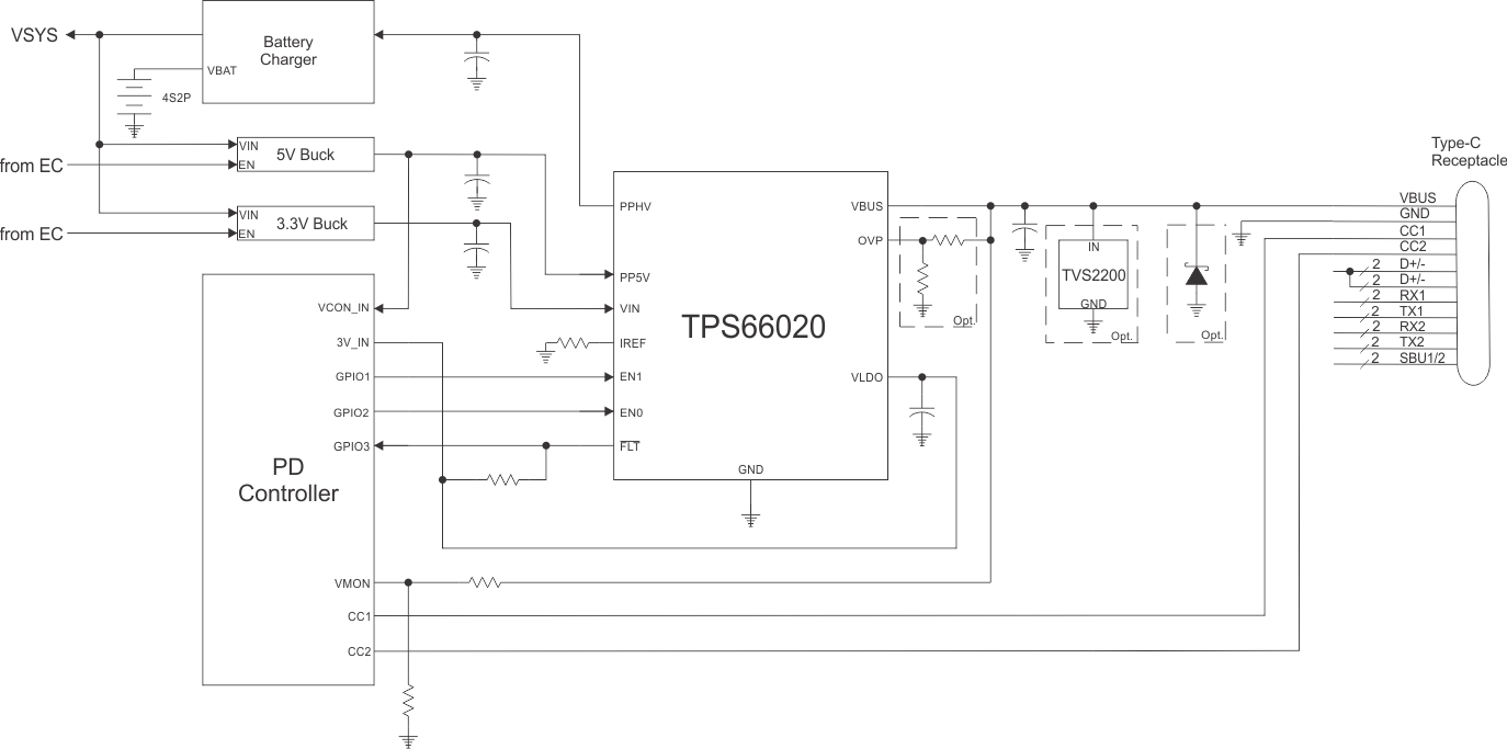
Similarly, Figure 29 shows a USB Type-C single port design using a PD controller that only supports 3.3-V operation. In this case, a separate 3.3-V supply in the system is used to supply power to the TPS66020. The TPS66020 supplies power to the 3.3-V supply of the PD controller via its VLDO output which is sourced either from the integrated 3.3-V VBUS LDO for dead battery operation or from VIN once the dead battery condition ends.
The PP5V integrated power path is used to provide 5-V VBUS power when the device is enabled as Source. The PPHV integrated power path provides power to the system and battery charger from VBUS when the device is enabled as a Sink.
 Figure 28. Single Port Type-C PD Port Using a Single 5-V Supply
  Figure 29. Single Port Type-C PD Port Using a 3.3-V Supply