SLVSCE6C December 2013 – June 2018 TPS709-Q1
PRODUCTION DATA.
- 1 Features
- 2 Applications
- 3 Description
- 4 Revision History
- 5 Pin Configuration and Functions
- 6 Specifications
- 7 Detailed Description
- 8 Application and Implementation
- 9 Power Supply Recommendations
- 10Layout
- 11Device and Documentation Support
- 12Mechanical, Packaging, and Orderable Information
Package Options
Refer to the PDF data sheet for device specific package drawings
Mechanical Data (Package|Pins)
- DBV|5
- DRV|6
Thermal pad, mechanical data (Package|Pins)
- DRV|6
Orderable Information
5 Pin Configuration and Functions
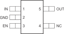
DBV Package
SOT-23-5
(Top View)

Pin Functions
| PIN | I/O | DESCRIPTION | ||
|---|---|---|---|---|
| NAME | NO. | |||
| DRV | DBV | |||
| EN | 4 | 3 | I | Enable pin. Driving this pin high enables the device. Driving this pin low puts the device into low current shutdown. This pin can be left floating to enable the device. The maximum voltage must remain below 6.5 V. |
| GND | 3 | 2 | — | Ground |
| IN | 6 | 1 | I | Unregulated input to the device |
| NC | 2, 5 | 4 | — | No internal connection |
| OUT | 1 | 5 | O | Regulated output voltage. Connect a small 2.2-µF or greater ceramic capacitor from this pin to ground to assure stability. |
| Thermal pad | — | — | The thermal pad is electrically connected to the GND node.
Connect to the GND plane for improved thermal performance. |
|
