SBVS128F June 2009 – December 2015 TPS727
PRODUCTION DATA.
- 1 Features
- 2 Applications
- 3 Description
- 4 Revision History
- 5 Pin Configurations and Functions
- 6 Specifications
- 7 Detailed Description
- 8 Applications and Implementation
- 9 Power-Supply Recommendations
- 10Layout
- 11Device and Documentation Support
- 12Mechanical, Packaging, and Orderable Information
Package Options
Refer to the PDF data sheet for device specific package drawings
Mechanical Data (Package|Pins)
- YFF|4
- DSE|6
Thermal pad, mechanical data (Package|Pins)
Orderable Information
8 Applications and Implementation
NOTE
Information in the following applications sections is not part of the TI component specification, and TI does not warrant its accuracy or completeness. TI’s customers are responsible for determining suitability of components for their purposes. Customers should validate and test their design implementation to confirm system functionality.
8.1 Application Information
The TPS727 family of low-dropout (LDO) linear regulators are utralow quiescent current LDOs with excellent line and ultra-fast load transient performance and are designed for power-sensitive applications.
8.2 Typical Application
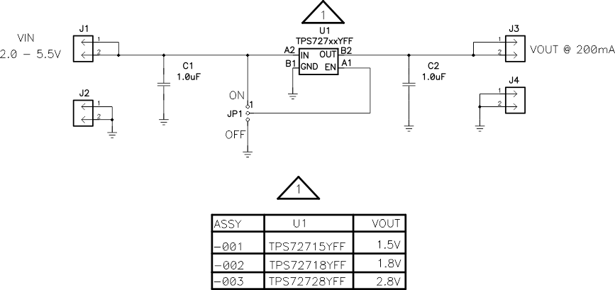 Figure 25. TPS72718YFF 2.5 VIN to 1.8 VOUT at 200 mA Schematic
8.2.1 Design Requirements
8.2.1.1 Input and Output Capacitor Requirements
Although an input capacitor is not required for stability, good analog design practice is to connect a 0.1-μF to
1.0-μF low equivalent series resistance (ESR) capacitor across the IN pin and GND input of the regulator. This capacitor counteracts reactive input sources and improves transient response, noise rejection, and ripple rejection. A higher-value capacitor may be necessary if large, fast rise-time load transients are anticipated, or if the device is not located close to the power source. If source impedance is not sufficiently low, a 0.1-μF input capacitor may be necessary to ensure stability.
The TPS727 is designed to be stable with standard ceramic capacitors with values of 1.0 μF or larger at the output. X5R- and X7R-type capacitors are best because they have minimal variation in value and ESR over temperature. Maximum ESR must be less than 200 mΩ.
8.2.1.2 Transient Response
As with any regulator, increasing the size of the output capacitor reduces over- and undershoot magnitude but increases duration of the transient response.
8.2.2 Detailed Design Procedure
Select the desired device based on the output voltage.
Provide an input supply with adequate headroom to include dropout and output current to account for the GND pin current and to power the load.
Select adequate input and output capacitors.
The startup current is given by Equation 2:

Equation 2 shows that soft-start current is directly proportional to COUT.
The output voltage ramp rate is independent of COUT and load current and has a typical value of 0.07 V/μs.
The TPS727 automatically adjusts the soft-start current to supply both the load current and the COUT charge current. For example, if ILOAD = 0 mA upon enabling the LDO, ISOFT START = 1 μF × 0.07 V/μs + 0 mA = 70 mA, the current that charges the output capacitor.
If ILOAD = 200 mA, ISOFT START = 1 μF × 0.07 V/μs + 200 mA = 270 mA, the current required for charging output capacitor and supplying the load current.
If the output capacitor and load are increased such that the soft-start current exceeds the output current limit, the current is clamped at the typical current limit of 400 mA. For example, if COUT = 10 μF and IOUT = 200 mA, 10 μF × 0.07 V/μs + 200 mA = 900 mA is not supplied. Instead, the current is clamped at 400 mA.
8.2.3 Application Curves
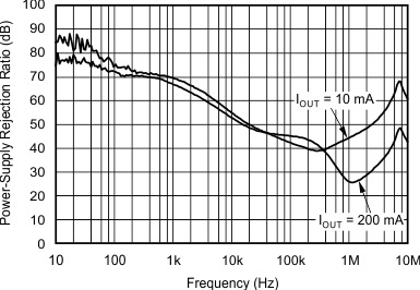
(VIN – VOUT = 0.5 V, TPS72718)
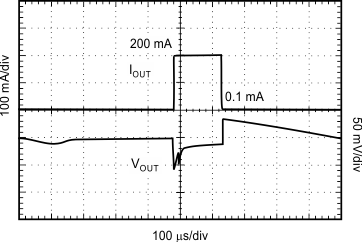
| VIN = 2.3 V, tR = tF = 1 µs |
(TPS72718)
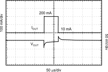
| VIN = 2.3 V, tR = tF = 1 µs |
(TPS72718)
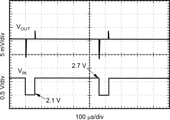
| Slew rate = 1 V/µs, IOUT = 200 µA |
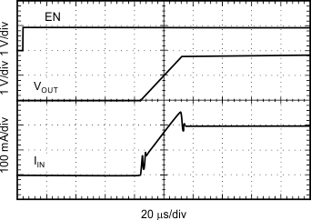
| VIN = 2.1 V, VOUT = 1.8 V, IOUT = 200 mA |
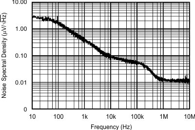
| IOUT = 10 mA, CIN = COUT = 1 µF |
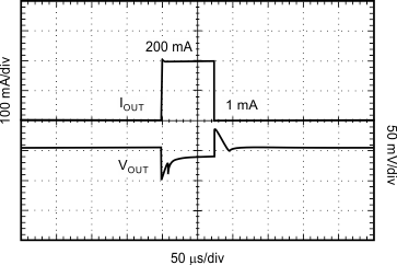
| VIN = 2.3 V, tR = tF = 1 µs |
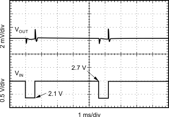
| Slew rate = 1 V/µs, IOUT = 100 µA |
| VIN = 2.1 V, VOUT = 1.8 V, IOUT = 100 µA |
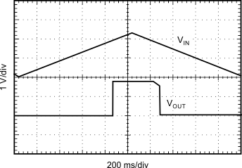
| IOUT = 200 mA |
8.3 Do's and Don'ts
Do place at least one 1.0-µF ceramic capacitor as close as possible to the OUT pin of the regulator.
Do not place the output capacitor more than 10 mm away from the regulator.
For DSE devices, do tie the NC pins to ground to improve thermal dissipation.
Do connect a 0.1-μF to 1.0-μF low equivalent series resistance (ESR) capacitor across the IN pin and GND input of the regulator.
Do not exceed the absolute maximum ratings.