SGLS303G May 2005 – December 2024 TPS732-Q1
PRODUCTION DATA
- 1
- 1 Features
- 2 Applications
- 3 Description
- 4 Pin Configuration and Functions
- 5 Specifications
- 6 Detailed Description
- 7 Application and Implementation
- 8 Device and Documentation Support
- 9 Revision History
- 10Mechanical, Packaging, and Orderable Information
Package Options
Mechanical Data (Package|Pins)
Thermal pad, mechanical data (Package|Pins)
Orderable Information
3 Description
The TPS732-Q1 low-dropout (LDO) voltage regulator uses san NMOS topology consisting of an NMOS pass transient in a voltage-follower configuration. This topology is stable using output capacitors with low ESR, and even allows operation without a capacitor. The topology also provides high reverse blockage (low reverse current) and ground pin current that is nearly constant over all values of output current.
The TPS732-Q1 uses an advanced BiCMOS process to yield high precision while delivering low dropout voltages and low ground pin current. Current consumption, when not enabled, is under 1μA and designed for portable applications. The extremely low output noise (30μVRMS with 0.1µF CNR) is designed for powering VCOs. This device is protected by thermal shutdown and foldback current limit.
| PART NUMBER | PACKAGE(1) | PACKAGE SIZE(2) |
|---|---|---|
| TPS732-Q1 | DBV (SOT-23, 5) | 2.9mm × 2.8mm |
| DCQ (SOT-223, 6) | 6.5mm × 7.06mm | |
| DRB (VSON, 8) | 3mm × 3mm |
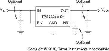
 Typical Application Circuit for Fixed Voltage Versions