SBVS252B October   2014  – February 2019 TPS735-Q1

PRODUCTION DATA.  

  1. Features
  2. Applications
  3. Description
    1.     Device Images
      1.      Typical Application
  4. Revision History
  5. Pin Configuration and Functions
    1.     Pin Functions
  6. Specifications
    1. 6.1 Absolute Maximum Ratings
    2. 6.2 ESD Ratings
    3. 6.3 Recommended Operating Conditions
    4. 6.4 Thermal Information
    5. 6.5 Electrical Characteristics
    6. 6.6 Typical Characteristics
  7. Detailed Description
    1. 7.1 Overview
    2. 7.2 Functional Block Diagram
    3. 7.3 Feature Description
      1. 7.3.1 Internal Current-Limit
      2. 7.3.2 Shutdown
      3. 7.3.3 Dropout Voltage
      4. 7.3.4 Startup and Noise Reduction Capacitor
      5. 7.3.5 Transient Response
      6. 7.3.6 Undervoltage Lockout (UVLO)
      7. 7.3.7 Minimum Load
    4. 7.4 Device Functional Modes
      1. 7.4.1 Normal Operation
      2. 7.4.2 Dropout Operation
      3. 7.4.3 Disabled
  8. Application and Implementation
    1. 8.1 Application Information
    2. 8.2 Typical Application
      1. 8.2.1 Design Requirements
        1. 8.2.1.1 Input and Output Capacitor Requirements
        2. 8.2.1.2 Feedback Capacitor Requirements (TPS73501-Q1 only)
      2. 8.2.2 Detailed Design Procedure
        1. 8.2.2.1 Output Noise
      3. 8.2.3 Application Curves
  9. Power Supply Recommendations
  10. 10Layout
    1. 10.1 Layout Guidelines
      1. 10.1.1 Board Layout Recommendations to Improve PSRR and Noise Performance
      2. 10.1.2 Thermal Protection
      3. 10.1.3 Package Mounting
      4. 10.1.4 Power Dissipation
      5. 10.1.5 Estimating Junction Temperature
    2. 10.2 Layout Example
  11. 11Device and Documentation Support
    1. 11.1 Device Support
      1. 11.1.1 Device Nomenclature
    2. 11.2 Documentation Support
      1. 11.2.1 Related Documentation
    3. 11.3 Receiving Notification of Documentation Updates
    4. 11.4 Community Resources
    5. 11.5 Trademarks
    6. 11.6 Electrostatic Discharge Caution
    7. 11.7 Glossary
  12. 12Mechanical, Packaging, and Orderable Information

Package Options

Mechanical Data (Package|Pins)
Thermal pad, mechanical data (Package|Pins)
Orderable Information

Application Curves

At VIN = VOUTnom + 0.5 V or 2.7 V (whichever is greater), IOUT = 1 mA, VEN = VIN, COUT = 2.2 μF, CNR = 0.01 μF, and TA = 25°C, unless otherwise noted.
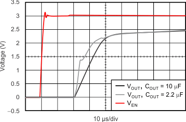
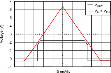
TPS735-Q1 tc_turn_on_resp_sbvs252.gif
Figure 17. TPS73525-Q1 Turn-On Response (VIN = VEN)
TPS735-Q1 tc_pupd_sbvs252.gif
RL = 5 Ω
Figure 19. TPS73525-Q1 Power-Up and Power-Down
(VIN = VEN)
TPS735-Q1 tc_line_tr_sbvs252.gif
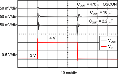
Figure 21. TPS73525-Q1 Line Transient Response
TPS735-Q1 tc_enable_resp_vin_sbvs252.gif
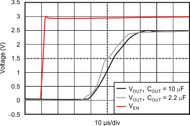
Figure 18. TPS73525-Q1 Turn-On Response Using EN
TPS735-Q1 tc_load_tr_sbvs252.gif
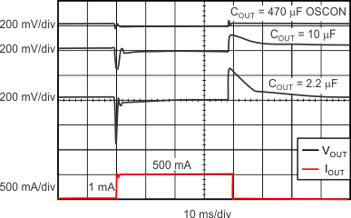
VIN = 3 V
Figure 20. TPS73525-Q1 Load Transient Response