SLVSAI3B September   2010  – December 2024 TPS736-Q1

PRODUCTION DATA  

  1.   1
  2. Features
  3. Applications
  4. Description
  5. Pin Configuration and Functions
  6. Specifications
    1. 5.1 Absolute Maximum Ratings
    2. 5.2 ESD Ratings
    3. 5.3 Recommended Operating Conditions
    4. 5.4 Thermal Information
    5. 5.5 Electrical Characteristics
    6. 5.6 Typical Characteristics
  7. Detailed Description
    1. 6.1 Overview
    2. 6.2 Functional Block Diagrams
    3. 6.3 Feature Description
      1. 6.3.1 Internal Current Limit
      2. 6.3.2 Transient Response
      3. 6.3.3 Reverse Current
      4. 6.3.4 Thermal Protection
    4. 6.4 Device Functional Modes
      1. 6.4.1 Enable Pin and Shutdown
      2. 6.4.2 Dropout Voltage
  8. Application and Implementation
    1. 7.1 Application Information
    2. 7.2 Typical Applications
      1. 7.2.1 Typical Application Circuit for Fixed-Voltage Versions
        1. 7.2.1.1 Design Requirements
        2. 7.2.1.2 Detailed Design Procedure
          1. 7.2.1.2.1 Input And Output Capacitor Requirements
          2. 7.2.1.2.2 Output Noise
        3. 7.2.1.3 Application Curves
      2. 7.2.2 Typical Application Circuit for Adjustable-Voltage Version
        1. 7.2.2.1 Design Requirements
    3. 7.3 Power Supply Recommendations
    4. 7.4 Layout
      1. 7.4.1 Layout Example
      2. 7.4.2 Thermal Considerations
      3. 7.4.3 Layout Guidelines
  9. Device And Documentation Support
    1. 8.1 Device Support
      1. 8.1.1 Device Nomenclature
    2. 8.2 Receiving Notification of Documentation Updates
    3. 8.3 Support Resources
    4. 8.4 Trademarks
    5. 8.5 Electrostatic Discharge Caution
    6. 8.6 Glossary
  10. Revision History
  11. 10Mechanical, Packaging, And Orderable Information

Package Options

Mechanical Data (Package|Pins)
Thermal pad, mechanical data (Package|Pins)
Orderable Information

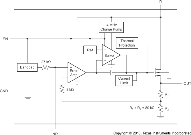
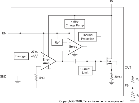
Functional Block Diagrams

TPS736-Q1 Fixed Voltage VersionFigure 6-1 Fixed Voltage Version
TPS736-Q1 Adjustable Voltage Version
See Table 6-1 for standard resistor values.
Figure 6-2 Adjustable Voltage Version
Table 6-1 Standard 1% Resistor Values for Common Output Voltages
VOUT(1) R1 R2
1.2V Short Open
1.5V 23.2kΩ 95.3kΩ
1.8V 28kΩ 56.2kΩ
2.5V 39.2kΩ 36.5kΩ
2.8V 44.2kΩ 33.2kΩ
3V 46.4kΩ 30.9kΩ
3.3V 52.3kΩ 30.1kΩ
VOUT = ( R1 + R2 ) / R2 × 1.204; R1 || R2 ≅ 19kΩ for best accuracy.