SLVSAI3A September 2010 – May 2016
PRODUCTION DATA.
- 1 Features
- 2 Applications
- 3 Description
- 4 Revision History
- 5 Pin Configuration and Functions
- 6 Specifications
- 7 Detailed Description
- 8 Application and Implementation
- 9 Power Supply Recommendations
- 10Layout
- 11Device And Documentation Support
- 12Mechanical, Packaging, And Orderable Information
Package Options
Mechanical Data (Package|Pins)
Thermal pad, mechanical data (Package|Pins)
Orderable Information
10 Layout
10.1 Layout Guidelines
Solder pad footprint recommendations for the TPS736xx-Q1 are presented in Solder Pad Recommendations for Surface-Mount Devices, SBFA015.
10.2 Layout Example
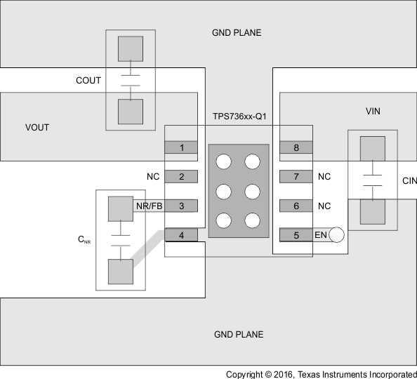
 Figure 35. Fixed-Output Voltage Option Layout
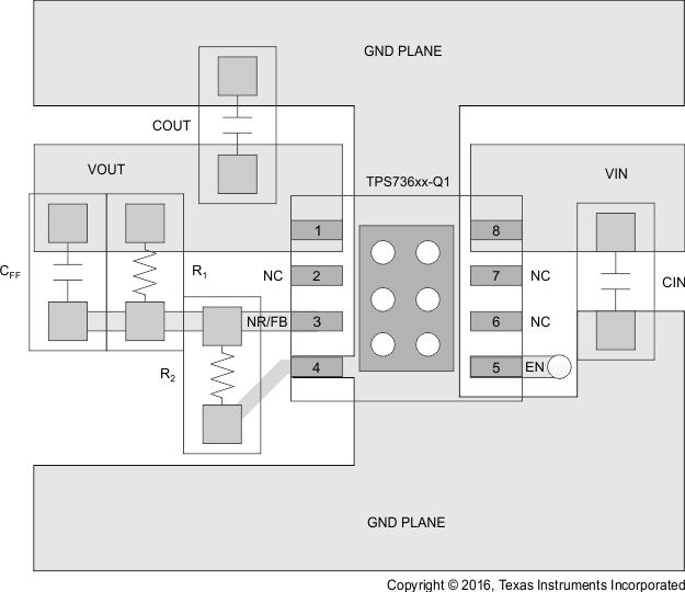
 Figure 36. Adjustable-Output Voltage Option Layout
10.3 Thermal Considerations
The ability to remove heat from the die is different for each package type, presenting different considerations in the PCB layout. The PCB area around the device that is free of other components moves the heat from the device to the ambient air. Performance data for JEDEC low- and high-K boards are shown in the Thermal Information table. Using heavier copper increases the effectiveness in removing heat from the device. The addition of plated through-holes to heat-dissipating layers also improve the heat sink effectiveness.
Power dissipation depends on input voltage and load conditions. Power dissipation (PD) is equal to the product of the output current times the voltage drop across the output pass element (VIN to VOUT), shown in Equation 6:

Power dissipation can be minimized by using the lowest possible input voltage necessary to assure the required output voltage.
10.4 Power Dissipation
To improve AC performance such as PSRR, output noise, and transient response, TI recommends that the board be designed with separate ground planes for VIN and VOUT, with each ground plane connected only at the GND pin of the device. In addition, the ground connection for the bypass capacitor must connect directly to the GND pin of the device.