SBVS067U January   2006  – September 2024 TPS737

PRODUCTION DATA  

  1.   1
  2. Features
  3. Applications
  4. Description
  5. Pin Configuration and Functions
  6. Specifications
    1. 5.1 Absolute Maximum Ratings
    2. 5.2 ESD Ratings
    3. 5.3 Recommended Operating Conditions
    4. 5.4 Thermal Information
    5. 5.5 Thermal Information
    6. 5.6 Electrical Characteristics
    7. 5.7 Typical Characteristics
  7. Detailed Description
    1. 6.1 Overview
    2. 6.2 Functional Block Diagrams
    3. 6.3 Feature Description
      1. 6.3.1 Output Noise
      2. 6.3.2 Internal Current Limit
      3. 6.3.3 Enable Pin and Shutdown
      4. 6.3.4 Reverse Current
    4. 6.4 Device Functional Modes
  8. Application and Implementation
    1. 7.1 Application Information
    2. 7.2 Typical Application
      1. 7.2.1 Design Requirements
      2. 7.2.2 Detailed Design Procedure
        1. 7.2.2.1 Input and Output Capacitor Requirements
        2. 7.2.2.2 Dropout Voltage
        3. 7.2.2.3 Transient Response
      3. 7.2.3 Application Curves
    3. 7.3 Best Design Practices
    4. 7.4 Power Supply Recommendations
    5. 7.5 Layout
      1. 7.5.1 Layout Guidelines
        1. 7.5.1.1 Power Dissipation
        2. 7.5.1.2 Thermal Protection
        3. 7.5.1.3 Estimating Junction Temperature
      2. 7.5.2 Layout Example
  9. Device and Documentation Support
    1. 8.1 Device Support
      1. 8.1.1 Development Support
        1. 8.1.1.1 Evaluation Modules
        2. 8.1.1.2 Spice Models
      2. 8.1.2 Device Nomenclature
    2. 8.2 Documentation Support
      1. 8.2.1 Related Documentation
    3. 8.3 Receiving Notification of Documentation Updates
    4. 8.4 Support Resources
    5. 8.5 Trademarks
    6. 8.6 Electrostatic Discharge Caution
    7. 8.7 Glossary
  10. Revision History
  11. 10Mechanical, Packaging, and Orderable Information

Package Options

Refer to the PDF data sheet for device specific package drawings

Mechanical Data (Package|Pins)
  • DCQ|6
  • DRV|6
  • DRB|8
Thermal pad, mechanical data (Package|Pins)
Orderable Information

Application Curves

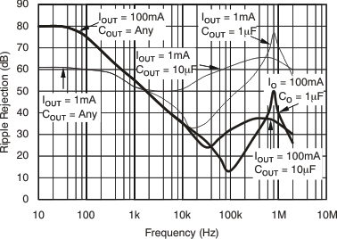
TPS737 PSRR
                        (Ripple Rejection) vs Frequency
Legacy silicon 
Figure 7-3 PSRR (Ripple Rejection) vs Frequency
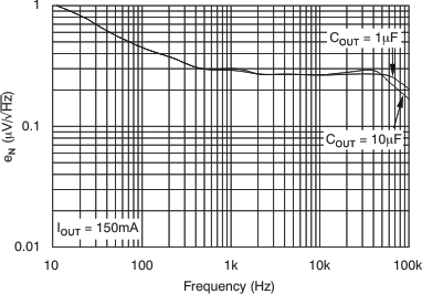
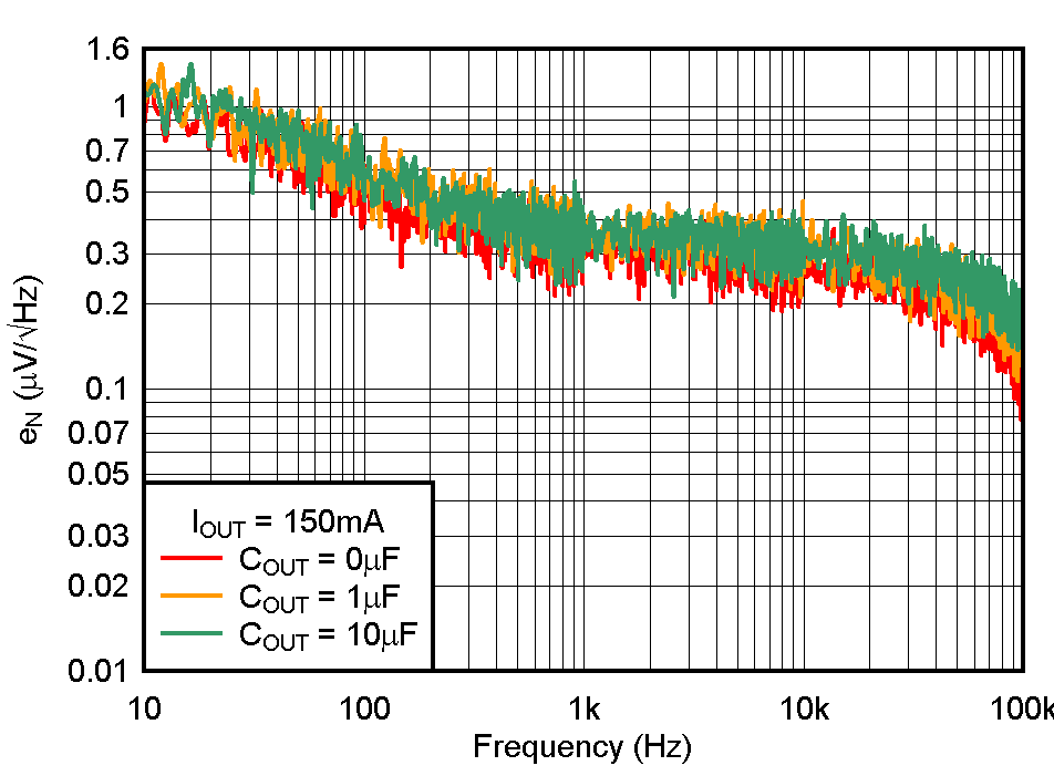
TPS737 Noise
                        Spectral Density
Legacy silicon 
Figure 7-5 Noise Spectral Density
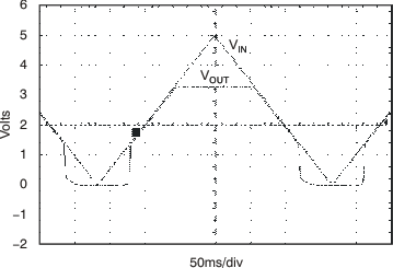
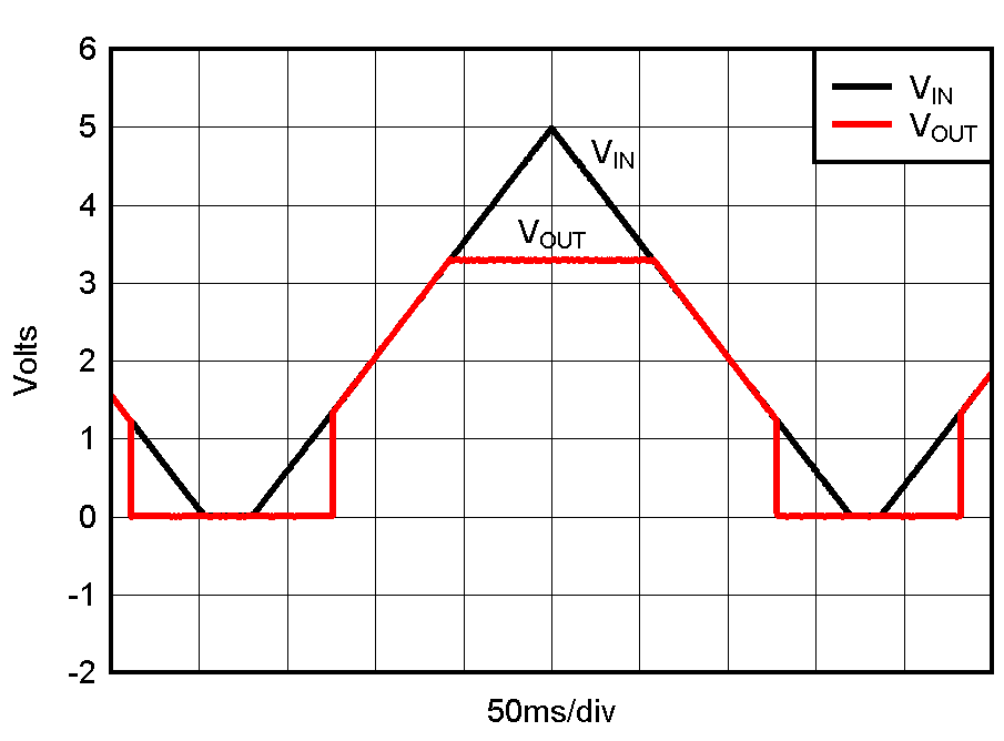
TPS737 TPS73701, VOUT = 3.3-V Power-Up and Power-Down
Legacy silicon 
Figure 7-7 TPS73701, VOUT = 3.3-V Power-Up and Power-Down
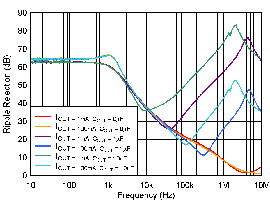
TPS737 PSRR
                        (Ripple Rejection) vs Frequency
New silicon
Figure 7-4 PSRR (Ripple Rejection) vs Frequency
TPS737 Noise
                        Spectral Density
New silicon 
Figure 7-6 Noise Spectral Density
TPS737 TPS73701, VOUT = 3.3-V Power-Up and Power-Down
New silicon
Figure 7-8 TPS73701, VOUT = 3.3-V Power-Up and Power-Down