SBVS064O December 2005 – October 2024 TPS74201
PRODUCTION DATA
- 1
- 1 Features
- 2 Applications
- 3 Description
- 4 Pin Configuration and Functions
- 5 Specifications
- 6 Detailed Description
- 7 Application and Implementation
- 8 Device and Documentation Support
- 9 Revision History
- 10Mechanical, Packaging, and Orderable Information
Package Options
Mechanical Data (Package|Pins)
Thermal pad, mechanical data (Package|Pins)
Orderable Information
4 Pin Configuration and Functions
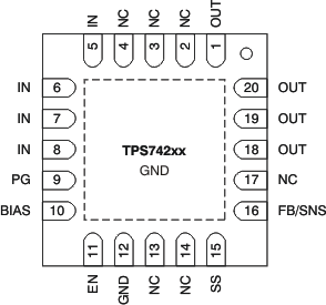
 Figure 4-1 RGW, RGR Packages20-Pin VQFN with Exposed Thermal PadTop View
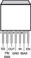
 Figure 4-2 KTW Package7-Pin DDPAK/TO-263Top View (legacy
chip only)
Figure 4-2 KTW Package7-Pin DDPAK/TO-263Top View (legacy
chip only)Table 4-1 Pin Functions
| PIN | Type(1) | DESCRIPTION | ||
|---|---|---|---|---|
| NAME | KTW(2) (DDPAK/ TO-263) |
RGW, RGR(2) (VQFN) | ||
| BIAS | 6 | 10 | I | Bias input voltage for error amplifier, reference, and internal control circuits. |
| EN | 7 | 11 | I | Enable pin. Driving this pin high enables the regulator. Driving this pin low puts the regulator into shutdown mode. This pin must not be left floating. |
| FB | 2 | 16 | I | This pin is the feedback connection to the center tap of an external resistor divider network that sets the output voltage. This pin must not be left floating. (Adjustable version only.) |
| GND | 4 | 12 | — | Ground |
| IN | 5 | 5,6,7,8 | I | Unregulated input to the device. |
| NC | — | 2, 3,4, 13,14,17 | O | No connection. This pin can be left floating or connected to GND to allow better thermal contact to the top-side plane. |
| OUT | 3 | 1, 18, 19, 20 | O | Regulated output voltage. No capacitor is required on this pin for stability. |
| PAD/TAB | — | — | — | Solder to the ground plane for increased thermal performance. |
| PG | — | 9 | O | Power-Good (PG) is an open-drain, active-high output that indicates the status of VOUT. When VOUT exceeds the PG trip threshold, the PG pin goes into a high-impedance state. When VOUT is below this threshold the pin is driven to a low-impedance state. Connect a pullup resistor from 10 kΩ to 1 MΩ from this pin to a supply up to 5.5 V. The supply can be higher than the input voltage. Alternatively, the PG pin can be left floating if output monitoring is not necessary. |
| SNS | 2 | 16 | I | This pin is the sense connection to the load device. This pin must be connected to VOUT and must not be left floating. (Fixed versions only.) |
| SS | 1 | 15 | — | Soft-Start pin. A capacitor connected on this pin to ground sets the start-up time. If this pin is left floating, the regulator output soft-start ramp time is typically 100 μs. |
(1) I = Input; O = Output;
(2) The RGR and KTW package are only for the legacy device.