SBVS064O December   2005  – October 2024 TPS74201

PRODUCTION DATA  

  1.   1
  2. Features
  3. Applications
  4. Description
  5. Pin Configuration and Functions
  6. Specifications
    1. 5.1 Absolute Maximum Ratings
    2. 5.2 ESD Ratings
    3. 5.3 Recommended Operating Conditions
    4. 5.4 Thermal Information
    5. 5.5 Electrical Characteristics
    6. 5.6 Typical Characteristics
  7. Detailed Description
    1. 6.1 Overview
    2. 6.2 Functional Block Diagram
    3. 6.3 Feature Description
      1. 6.3.1 Enable and Shutdown
      2. 6.3.2 Power-Good (VQFN Packages Only)
      3. 6.3.3 Internal Current Limit
    4. 6.4 Device Functional Modes
      1. 6.4.1 Normal Operation
      2. 6.4.2 Dropout Operation
      3. 6.4.3 Disabled
  8. Application and Implementation
    1. 7.1 Application Information
      1. 7.1.1 Input, Output, and Bias Capacitor Requirements
      2. 7.1.2 Transient Response
      3. 7.1.3 Dropout Voltage
      4. 7.1.4 Output Noise
      5. 7.1.5 Programmable Soft-Start
      6. 7.1.6 Sequencing Requirements
    2. 7.2 Typical Applications
      1. 7.2.1 Design Requirements
      2. 7.2.2 Detailed Design Procedure
      3. 7.2.3 Application Curves
    3. 7.3 Power Supply Recommendations
    4. 7.4 Layout
      1. 7.4.1 Layout Guidelines
      2. 7.4.2 Layout Example
      3. 7.4.3 Thermal Protection
      4. 7.4.4 Thermal Considerations
  9. Device and Documentation Support
    1. 8.1 Device Support
      1. 8.1.1 Development Support
        1. 8.1.1.1 Evaluation Modules
        2. 8.1.1.2 Spice Models
    2. 8.2 Documentation Support
      1. 8.2.1 Related Documentation
      2. 8.2.2 Device Nomenclature
    3. 8.3 Receiving Notification of Documentation Updates
    4. 8.4 Support Resources
    5. 8.5 Trademarks
    6. 8.6 Electrostatic Discharge Caution
    7. 8.7 Glossary
  10. Revision History
  11. 10Mechanical, Packaging, and Orderable Information

Package Options

Mechanical Data (Package|Pins)
Thermal pad, mechanical data (Package|Pins)
Orderable Information

Application Curves

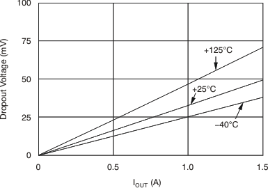
TPS74201 VIN Dropout Voltage vs  IOUT and Temperature (TJ)Figure 7-5 VIN Dropout Voltage vs IOUT and Temperature (TJ)
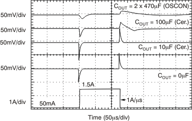
TPS74201 Output Load Transient ResponseFigure 7-7 Output Load Transient Response
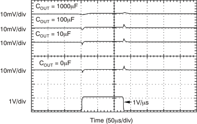
TPS74201 VBIAS Line Transient (1.5 A)
Figure 7-6 VBIAS Line Transient (1.5 A)
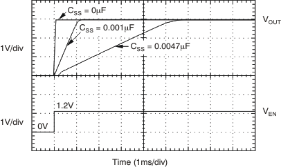
TPS74201 Turnon ResponseFigure 7-8 Turnon Response