SBVS064O December 2005 – October 2024 TPS74201
PRODUCTION DATA
- 1
- 1 Features
- 2 Applications
- 3 Description
- 4 Pin Configuration and Functions
- 5 Specifications
- 6 Detailed Description
- 7 Application and Implementation
- 8 Device and Documentation Support
- 9 Revision History
- 10Mechanical, Packaging, and Orderable Information
Package Options
Mechanical Data (Package|Pins)
Thermal pad, mechanical data (Package|Pins)
Orderable Information
7.1.6 Sequencing Requirements
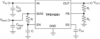
The device can have VIN, VBIAS, and VEN sequenced in any order without causing damage to the device. However, for the soft-start function to work as intended, certain sequencing rules must be applied. Enabling the device after VIN and VBIAS are present is preferred, and can be accomplished using a digital output from a processor or supply supervisor. An analog signal from an external RC circuit, as shown in Figure 7-3, can also be used as long as the delay time is long enough for VIN and VBIAS to be present.
 Figure 7-3 Soft-Start Delay Using an RC Circuit on Enable
If a signal is not available to enable the device after IN and BIAS, simply connecting EN to IN is acceptable for most applications as long as VIN is greater than 1.1 V and the ramp rate of VIN and VBIAS is faster the set soft-start ramp rate. If the ramp rate of the input sources is slower than the set soft-start time, the output tracks the slower supply minus the dropout voltage until the set output voltage is reached. If EN is connected to BIAS, the device does soft-start as programmed provided that VIN is present before VBIAS. If VBIAS and VEN are present before VIN is applied and the set soft-start time has expired then VOUT tracks VIN.
When VBIAS and VEN are present and VIN is not supplied, this device outputs approximately 50 μA of current from OUT. Although this condition does not cause any damage to the device, the output current can charge up the OUT node if total resistance between OUT and GND (including external feedback resistors) is greater than 10 kΩ.