SBVS337A April   2018  – December 2018 TPS746

PRODUCTION DATA.  

  1. Features
  2. Applications
  3. Description
    1.     Device Images
      1.      Typical Application
  4. Revision History
  5. Pin Configuration and Functions
    1.     Pin Functions
  6. Specifications
    1. 6.1 Absolute Maximum Ratings
    2. 6.2 ESD Ratings
    3. 6.3 Recommended Operating Conditions
    4. 6.4 Thermal Information
    5. 6.5 Electrical Characteristics
    6. 6.6 Timing Requirements
    7. 6.7 Typical Characteristics
  7. Detailed Description
    1. 7.1 Overview
    2. 7.2 Functional Block Diagram
    3. 7.3 Feature Description
      1. 7.3.1 Undervoltage Lockout (UVLO)
      2. 7.3.2 Shutdown
      3. 7.3.3 Foldback Current Limit
      4. 7.3.4 Thermal Shutdown
    4. 7.4 Device Functional Modes
      1. 7.4.1 Device Functional Mode Comparison
      2. 7.4.2 Normal Operation
      3. 7.4.3 Dropout Operation
      4. 7.4.4 Disabled
  8. Application and Implementation
    1. 8.1 Application Information
      1. 8.1.1 Adjustable Device Feedback Resistors
      2. 8.1.2 Input and Output Capacitor Selection
      3. 8.1.3 Dropout Voltage
      4. 8.1.4 Exiting Dropout
      5. 8.1.5 Reverse Current
      6. 8.1.6 Power Dissipation (PD)
      7. 8.1.7 Power-Good Function
    2. 8.2 Feed-Forward Capacitor (CFF)
    3. 8.3 Typical Application
      1. 8.3.1 Design Requirements
      2. 8.3.2 Detailed Design Procedure
        1. 8.3.2.1 Input Current
        2. 8.3.2.2 Thermal Dissipation
      3. 8.3.3 Application Curve
  9. Power Supply Recommendations
  10. 10Layout
    1. 10.1 Layout Guidelines
    2. 10.2 Layout Example
  11. 11Device and Documentation Support
    1. 11.1 Documentation Support
      1. 11.1.1 Related Documentation
    2. 11.2 Receiving Notification of Documentation Updates
    3. 11.3 Community Resources
    4. 11.4 Trademarks
    5. 11.5 Electrostatic Discharge Caution
    6. 11.6 Glossary
  12. 12Mechanical, Packaging, and Orderable Information

Package Options

Mechanical Data (Package|Pins)
Thermal pad, mechanical data (Package|Pins)
Orderable Information

Adjustable Device Feedback Resistors

Figure 46 shows that the output voltage of the TPS746 can be adjusted from 0.55 V to 5.5 V by using a resistor divider network.
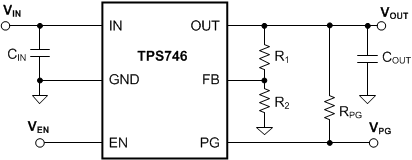
TPS746 simpschem_TPS746.gifFigure 46. Adjustable Operation

The adjustable-version device requires external feedback divider resistors to set the output voltage. VOUT is set using the feedback divider resistors, R1 and R2, according to the following equation:

Equation 2. VOUT = VFB × (1 + R1 / R2)

For this device, VFB = 0.55 V.

To ignore the FB pin current error term in the VOUT equation, set the feedback divider current to 100x the FB pin current listed in the Electrical Characteristics table. This setting provides the maximum feedback divider series resistance, as shown in the following equation:

Equation 3. R1 + R2 ≤ VOUT / (IFB × 100)

For this device, IFB = 10 nA.