SBVS099H november   2007  – april 2023 TPS74701

PRODUCTION DATA  

  1. Features
  2. Applications
  3. Description
  4. Revision History
  5. Pin Configuration and Functions
  6. Specifications
    1. 6.1  Absolute Maximum Ratings
    2. 6.2  ESD Ratings
    3. 6.3  Recommended Operating Conditions
    4. 6.4  Thermal Information
    5. 6.5  Electrical Characteristics: Other Orderable Devices (non-M3 Suffix)
    6. 6.6  Electrical Characteristics: Orderable Device (M3 Suffix)
    7. 6.7  Typical Characteristics: VEN = VIN (All Other Orderable Devices, Non-M3 Suffix)
    8. 6.8  Typical Characteristics: VEN = VIN = 1.8 V, VOUT = 1.5 V (All Other Orderable Devices, Non-M3 Suffix)
    9. 6.9  Typical Characteristics: IOUT = 50 mA (M3 Suffix)
    10. 6.10 Typical Characteristics: VEN = VIN = 1.8 V, VOUT = 1.5 V (M3 Suffix)
  7. Detailed Description
    1. 7.1 Overview
    2. 7.2 Functional Block Diagram
    3. 7.3 Feature Description
      1. 7.3.1 Programmable Soft-Start
      2. 7.3.2 Enable and Shutdown
      3. 7.3.3 Power Good
      4. 7.3.4 Internal Current Limit
      5. 7.3.5 Thermal Shutdown
    4. 7.4 Device Functional Modes
      1. 7.4.1 Normal Operation
      2. 7.4.2 Dropout Operation
      3. 7.4.3 Disabled
  8. Application and Implementation
    1. 8.1 Application Information
      1. 8.1.1 Input, Output, and Bias Capacitor Requirements
      2. 8.1.2 Transient Response
      3. 8.1.3 Dropout Voltage
      4. 8.1.4 Sequencing Requirements
      5. 8.1.5 Output Noise
    2. 8.2 Typical Application
      1. 8.2.1 Design Requirements
      2. 8.2.2 Detailed Design Procedure
      3. 8.2.3 Application Curves
    3. 8.3 Power Supply Recommendations
    4. 8.4 Layout
      1. 8.4.1 Layout Guidelines
        1. 8.4.1.1 Power Dissipation
        2. 8.4.1.2 Estimating Junction Temperature
      2. 8.4.2 Layout Example
  9. Device and Documentation Support
    1. 9.1 Device Support
      1. 9.1.1 Development Support
        1. 9.1.1.1 Evaluation Module
        2. 9.1.1.2 Spice Models
      2. 9.1.2 Device Nomenclature
    2. 9.2 Documentation Support
      1. 9.2.1 Related Documentation
    3. 9.3 Receiving Notification of Documentation Updates
    4. 9.4 Support Resources
    5. 9.5 Trademarks
    6. 9.6 Electrostatic Discharge Caution
    7. 9.7 Glossary
  10. 10Mechanical, Packaging, and Orderable Information

Package Options

Mechanical Data (Package|Pins)
Thermal pad, mechanical data (Package|Pins)
Orderable Information

Typical Characteristics: VEN = VIN (All Other Orderable Devices, Non-M3 Suffix)

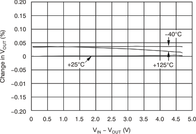
at TJ = 25°C, VIN = VOUT(TYP) + 0.3 V, VBIAS = 5 V, IOUT = 50 mA, VEN = VIN, CIN = 1 μF, CBIAS = 4.7 μF, and COUT = 10 μF (unless otherwise noted)
GUID-3C4CCFFB-23CA-489D-8B24-DA2CCFCC384A-low.gif
 
Figure 6-1 VIN Line Regulation
GUID-D5D6292D-DF3E-437D-8F59-5EC9035DBAE6-low.gif
 
Figure 6-3 Load Regulation
GUID-4D2B801B-9EEF-4A87-BD36-D83BD595C40B-low.gif
 
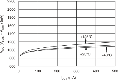
Figure 6-5 Dropout Voltage vs IOUT and Temperature (TJ)
GUID-5015071E-5C93-4257-8745-520B1E0D4C7F-low.gif
 
Figure 6-7 VBIAS Dropout Voltage vs IOUT and Temperature (TJ)
GUID-D7BB86A2-65DD-4444-8BEB-18C834FFB9AF-low.gif
 
Figure 6-9 VIN PSRR vs Frequency
GUID-1E07D0B6-F0F4-4C65-9F77-4E18511DE5DC-low.gif
 
Figure 6-11 Noise Spectral Density
GUID-97874AB1-5168-4612-BCF4-E246DC8EFD40-low.gif
 
Figure 6-13 BIAS Pin Current vs VBIAS and Temperature (TJ)
GUID-309E5D88-156D-4E49-A004-F67E58E4670D-low.gif
 
Figure 6-15 Low-Level PG Voltage vs Current
GUID-C7B00161-3E4C-41E9-9C43-45C1CA262D68-low.gif
 
Figure 6-2 VBIAS Line Regulation
GUID-607BEA88-EE20-4B5C-AB37-0FA678D0C9BB-low.gif
 
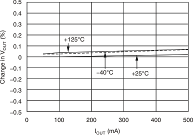
Figure 6-4 Load Regulation
GUID-CCF38E4C-F3B4-47DA-9DF4-9F8BAD09CA7D-low.gif
 
Figure 6-6 Dropout Voltage vs (VBIAS – VOUT) and Temperature (TJ)
GUID-47F36789-A6D2-4F98-8EA1-65AD655FDF61-low.gif
 
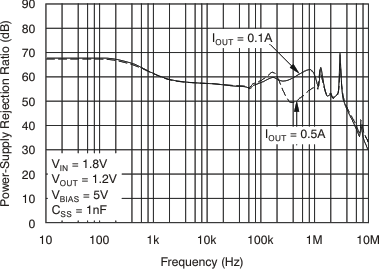
Figure 6-8 VBIAS PSRR vs Frequency
GUID-85428932-FB42-4A55-8344-70B87BC3DD6E-low.gif
 
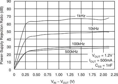
Figure 6-10 VIN PSRR vs (VIN – VOUT)
GUID-D574ECFC-6DD8-4054-8728-2EDAE8CEEC16-low.gif
 
Figure 6-12 BIAS Pin Current vs IOUT and Temperature (TJ)
GUID-EFE736EF-D2B5-4EC4-BB75-B8CF5A02EE8B-low.gif
 
Figure 6-14 Soft-Start Charging Current (ISS) vs Temperature (TJ)
GUID-567A9F94-384B-4F53-A68E-D8E1C238F669-low.gif
 
Figure 6-16 Current Limit vs (VBIAS – VOUT)