SBVS074N January   2007  – June 2024

PRODUCTION DATA  

  1.   1
  2. Features
  3. Applications
  4. Description
  5. Pin Configuration and Functions
  6. Specifications
    1. 5.1 Absolute Maximum Ratings
    2. 5.2 ESD Ratings
    3. 5.3 Recommended Operating Conditions
    4. 5.4 Thermal Information
    5. 5.5 Electrical Characteristics
    6. 5.6 Typical Characteristics: IOUT = 50 mA
    7. 5.7 Typical Characteristics: IOUT = 1 A
  7. Detailed Description
    1. 6.1 Overview
    2. 6.2 Functional Block Diagrams
    3. 6.3 Feature Description
      1. 6.3.1 Enable/Shutdown
      2. 6.3.2 Power Good
      3. 6.3.3 Internal Current Limit
      4. 6.3.4 Thermal Protection
    4. 6.4 Device Functional Modes
      1. 6.4.1 Normal Operation
      2. 6.4.2 Dropout Operation
      3. 6.4.3 Disabled
    5. 6.5 Programming
      1. 6.5.1 Programmable Soft-Start
      2. 6.5.2 Sequencing Requirements
  8. Application and Implementation
    1. 7.1 Application Information
      1. 7.1.1 Adjusting the Output Voltage
      2. 7.1.2 Input, Output, and Bias Capacitor Requirements
      3. 7.1.3 Transient Response
      4. 7.1.4 Dropout Voltage
      5. 7.1.5 Output Noise
    2. 7.2 Typical Applications
      1. 7.2.1 FPGA I/O Supply at 1.5 V With a Bias Rail
        1. 7.2.1.1 Design Requirements
        2. 7.2.1.2 Detailed Design Procedure
        3. 7.2.1.3 Application Curves
      2. 7.2.2 FPGA I/O Supply at 1.5 V Without a Bias Rail
        1. 7.2.2.1 Design Requirements
        2. 7.2.2.2 Detailed Design Procedure
        3. 7.2.2.3 Application Curves
    3. 7.3 Power Supply Recommendations
    4. 7.4 Layout
      1. 7.4.1 Layout Guidelines
        1. 7.4.1.1 Estimating Junction Temperature
      2. 7.4.2 Layout Example
  9. Device and Documentation Support
    1. 8.1 Device Support
      1. 8.1.1 Device Nomenclature
      2. 8.1.2 Development Support
        1. 8.1.2.1 Evaluation Modules
        2. 8.1.2.2 Spice Models
    2. 8.2 Documentation Support
      1. 8.2.1 Related Documentation
    3. 8.3 Receiving Notification of Documentation Updates
    4. 8.4 Support Resources
    5. 8.5 Trademarks
    6. 8.6 Electrostatic Discharge Caution
    7. 8.7 Glossary
  10. Revision History
  11. 10Mechanical, Packaging, and Orderable Information

Package Options

Mechanical Data (Package|Pins)
Thermal pad, mechanical data (Package|Pins)
Orderable Information

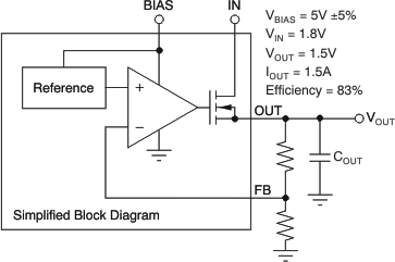
FPGA I/O Supply at 1.5 V With a Bias Rail

TPS748 Typical Application of the TPS748 Using an Auxiliary Bias RailFigure 7-2 Typical Application of the TPS748 Using an Auxiliary Bias Rail