SBVS082K June 2007 – June 2024 TPS74901
PRODUCTION DATA
- 1
- 1 Features
- 2 Applications
- 3 Description
- 4 Pin Configuration and Functions
- 5 Specifications
- 6 Detailed Description
- 7 Application and Implementation
- 8 Device and Documentation Support
- 9 Revision History
- 10Mechanical, Packaging, and Orderable Information
Package Options
Mechanical Data (Package|Pins)
Thermal pad, mechanical data (Package|Pins)
Orderable Information
7.2 Typical Application
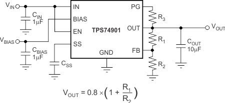
Figure 7-4 shows the typical application circuit for the TPS74901 adjustable output device.
R1 and R2 can be calculated for any output voltage using the formula shown in Figure 7-4. Table 7-2 lists sample resistor values of common output voltages. To achieve the maximum accuracy specifications, R2 must be ≤ 4.99kΩ.
 Figure 7-4 Typical Application Circuit for the TPS74901 (Adjustable)
Table 7-2 Standard 1% Resistor Values
for Programming the Output Voltage(1)
| R1 (kΩ) | R2 (kΩ) | VOUT (V) |
|---|---|---|
| Short | Open | 0.8 |
| 0.619 | 4.99 | 0.9 |
| 1.13 | 4.53 | 1 |
| 1.37 | 4.42 | 1.05 |
| 1.87 | 4.99 | 1.1 |
| 2.49 | 4.99 | 1.2 |
| 4.12 | 4.75 | 1.5 |
| 3.57 | 2.87 | 1.8 |
| 3.57 | 1.69 | 2.5 |
| 3.57 | 1.15 | 3.3 |
(1) VOUT = 0.8 × (1 + R1 / R2).