SLVS237E August   1999  – March 2024 TPS766

PRODUCTION DATA  

  1.   1
  2. Features
  3. Applications
  4. Description
  5. Pin Configuration and Functions
  6. Specifications
    1. 5.1 Absolute Maximum Ratings
    2. 5.2 ESD Ratings
    3. 5.3 Recommended Operating Conditions
    4. 5.4 Thermal Information (Legacy Chip)
    5. 5.5 Thermal Information (New Chip)
    6. 5.6 Electrical Characteristics
    7. 5.7 Timing Diagram
    8. 5.8 Typical Characteristics
    9. 5.9 Typical Characteristics: Supported ESR Range
  7. Detailed Description
    1. 6.1 Overview
    2. 6.2 Functional Block Diagrams
    3. 6.3 Feature Description
      1. 6.3.1 Output Enable
      2. 6.3.2 Dropout Voltage
      3. 6.3.3 Current Limit
      4. 6.3.4 Undervoltage Lockout (UVLO)
      5. 6.3.5 Power-Good Function
      6. 6.3.6 Output Pulldown
      7. 6.3.7 Thermal Shutdown
    4. 6.4 Device Functional Modes
      1. 6.4.1 Device Functional Mode Comparison
      2. 6.4.2 Normal Operation
      3. 6.4.3 Dropout Operation
      4. 6.4.4 Disabled
  8. Application and Implementation
    1. 7.1 Application Information
    2. 7.2 Typical Application
      1. 7.2.1 Design Requirements
      2. 7.2.2 Detailed Design Procedure
        1. 7.2.2.1 Adjustable Device Feedback Resistors
        2. 7.2.2.2 Recommended Capacitor Types
        3. 7.2.2.3 Input and Output Capacitor Requirements
        4. 7.2.2.4 Reverse Current
        5. 7.2.2.5 Feed-Forward Capacitor (CFF)
        6. 7.2.2.6 Power Dissipation (PD)
        7. 7.2.2.7 Estimating Junction Temperature
      3. 7.2.3 Application Curves
    3. 7.3 Power Supply Recommendations
    4. 7.4 Layout
      1. 7.4.1 Layout Guidelines
      2. 7.4.2 Layout Example
  9. Device and Documentation Support
    1. 8.1 Documentation Support
      1. 8.1.1 Device Nomenclature
    2. 8.2 Receiving Notification of Documentation Updates
    3. 8.3 Support Resources
    4. 8.4 Trademarks
    5. 8.5 Electrostatic Discharge Caution
    6. 8.6 Glossary
  10. Revision History
  11. 10Mechanical, Packaging, and Orderable Information

Package Options

Refer to the PDF data sheet for device specific package drawings

Mechanical Data (Package|Pins)
  • D|8
Thermal pad, mechanical data (Package|Pins)
Orderable Information

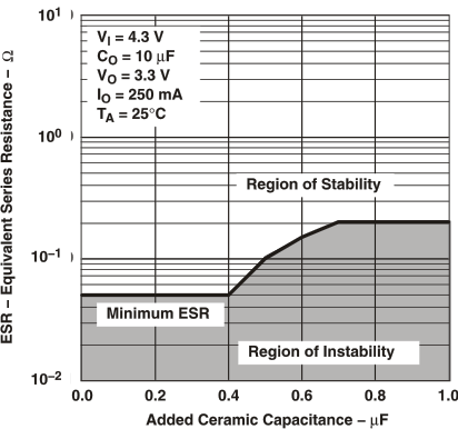
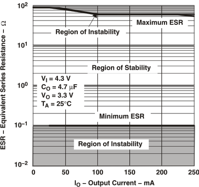
Typical Characteristics: Supported ESR Range

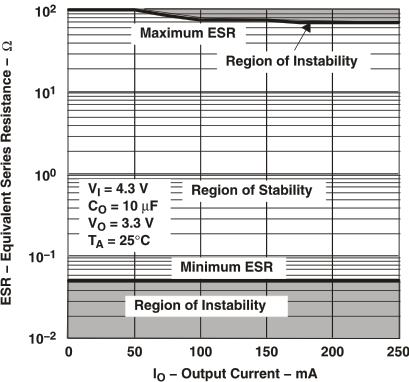
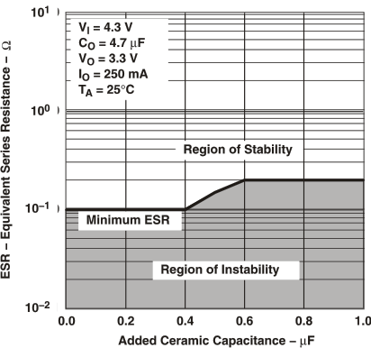
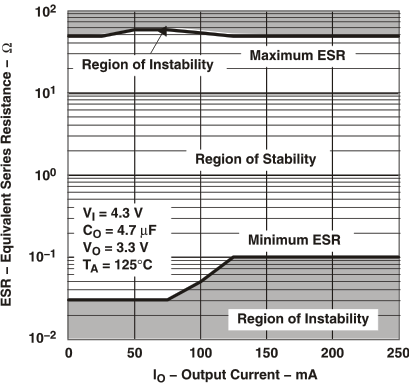
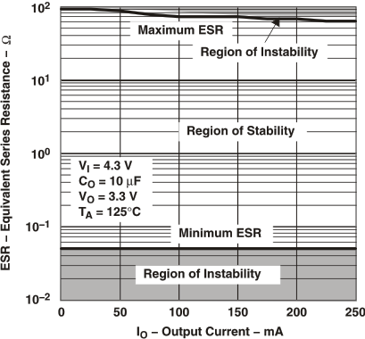
Equivalent series resistance (ESR) refers to the total series resistance, including the ESR of the capacitor, any series resistance added externally, and PCB trace resistance to CO. The setup shown in the Timing Diagram section characterizes the ESR behavior across temperature.
GUID-3D1B0309-5649-480D-B789-F651CF41BCCA-low.gif
 
Figure 5-47 Typical Region of Stability ESR vs Output Current (Legacy Chip)
GUID-20231201-SS0I-5TS5-SGWW-3W6PNBPRTXZL-low.svg
 
Figure 5-49 Typical Region of Stability ESR vs Output Current (New Chip)
GUID-20231201-SS0I-4Z1K-2FPD-53JMSKNT2GNP-low.svg
 
Figure 5-51 Typical Region of Stability ESR vs Output Current (New Chip)
GUID-FB3E606B-89AD-44D5-9662-1DAC46EDE13F-low.gif
 
Figure 5-53 Typical Region of Stability ESR vs Output Current (Legacy Chip)
GUID-20231201-SS0I-H3B0-PKQL-T2X6SXQ7HXN3-low.svg
 
Figure 5-55 Typical Region of Stability ESR vs Output Current (New Chip)
GUID-20231201-SS0I-3PM6-3LQ9-Z0HHLBNG77HK-low.svg
 
Figure 5-57 Typical Region of Stability ESR vs Output Current (New Chip)
GUID-20231201-SS0I-HZQX-9P69-ZMTGVRFG5K9S-low.svg
 
Figure 5-59 Typical Region of Stability ESR vs Output Current (New Chip)
GUID-20231201-SS0I-51N5-QXCP-SPQDDQXH2WDW-low.svg
 
Figure 5-61 Typical Region of Stability ESR vs Output Current (New Chip)
GUID-B0E0DF1C-0683-4526-B6FD-24E36049339D-low.gif
 
Figure 5-63 Typical Region of Stability ESR vs Added Ceramic Capacitance (Legacy Chip)
GUID-20231201-SS0I-W9NC-GX1Q-LKP0KKZQHLWS-low.svg
 
Figure 5-48 Typical Region of Stability ESR vs Output Current (New Chip)
GUID-D286547A-A69B-4547-97D5-A6BC5BDD2580-low.gif
 
Figure 5-50 Typical Region of Stability ESR vs Output Current (Legacy Chip)
GUID-20231201-SS0I-PPNV-ZVZ5-L6GK4MJVGM19-low.svg
 
Figure 5-52 Typical Region of Stability ESR vs Output Current (New Chip)
GUID-20231201-SS0I-XXC8-S8LV-5BNRFVKJDGX4-low.svg
 
Figure 5-54 Typical Region of Stability ESR vs Output Current (New Chip)
GUID-0696E88B-7AFF-4D66-909F-B54EE3216E6B-low.gif
 
Figure 5-56 Typical Region of Stability ESR vs Output Current (Legacy Chip)
GUID-20231201-SS0I-ZZF4-KFJF-BFSM3FBCDTJR-low.svg
 
Figure 5-58 Typical Region of Stability ESR vs Output Current (New Chip)
GUID-20231201-SS0I-WK0Q-LG9G-PNXHBJWJ4CXB-low.svg
 
Figure 5-60 Typical Region of Stability ESR vs Output Current (Legacy Chip)
GUID-20231201-SS0I-VST5-LTKQ-QWFTHK8CTFLH-low.svg
 
Figure 5-62 Typical Region of Stability ESR vs Output Current (New Chip)
GUID-BD9BADC0-95EA-4708-B600-22602EA0F2A7-low.gif
 
Figure 5-64 Typical Region of Stability ESR vs Added Ceramic Capacitance (Legacy Chip)