SGLS118E December   2001  – July 2024 TPS769-Q1

PRODUCTION DATA  

  1.   1
  2. Features
  3. Applications
  4. Description
  5. Pin Configuration and Functions
  6. Specifications
    1. 5.1 Absolute Maximum Ratings
    2. 5.2 ESD Ratings
    3. 5.3 Recommended Operating Conditions
    4. 5.4 Thermal Information
    5. 5.5 Dissipation Ratings (Legacy Chip)
    6. 5.6 Electrical Characteristics
    7. 5.7 Typical Characteristics
    8. 5.8 Typical Characteristics: Supported ESR Range
  7. Detailed Description
    1. 6.1 Overview
    2. 6.2 Functional Block Diagrams
    3. 6.3 Feature Description
      1. 6.3.1 Output Enable
      2. 6.3.2 Dropout Voltage
      3. 6.3.3 Current Limit
      4. 6.3.4 Undervoltage Lockout (UVLO)
      5. 6.3.5 Output Pulldown
      6. 6.3.6 Thermal Shutdown
    4. 6.4 Device Functional Modes
      1. 6.4.1 Normal Operation
      2. 6.4.2 Dropout Operation
      3. 6.4.3 Disabled
  8. Application and Implementation
    1. 7.1 Application Information
    2. 7.2 Typical Application
      1. 7.2.1 Design Requirements
      2. 7.2.2 Detailed Design Procedure
        1. 7.2.2.1 Adjustable Device Feedback Resistors
        2. 7.2.2.2 Recommended Capacitor Types
        3. 7.2.2.3 Input and Output Capacitor Requirements
        4. 7.2.2.4 Reverse Current
        5. 7.2.2.5 Feed-Forward Capacitor (CFF)
        6. 7.2.2.6 Power Dissipation (PD)
        7. 7.2.2.7 Estimating Junction Temperature
      3. 7.2.3 Application Curves
    3. 7.3 Power Supply Recommendations
    4. 7.4 Layout
      1. 7.4.1 Layout Guidelines
      2. 7.4.2 Layout Example
  9. Device and Documentation Support
    1. 8.1 Device Support
      1. 8.1.1 Development Support
        1. 8.1.1.1 Evaluation Module
        2. 8.1.1.2 Spice Models
        3. 8.1.1.3 Device Nomenclature
    2. 8.2 Documentation Support
      1. 8.2.1 Related Documentation
    3. 8.3 Receiving Notification of Documentation Updates
    4. 8.4 Support Resources
    5. 8.5 Trademarks
    6. 8.6 Electrostatic Discharge Caution
    7. 8.7 Glossary
  10. Revision History
  11. 10Mechanical, Packaging, and Orderable Information

Package Options

Refer to the PDF data sheet for device specific package drawings

Mechanical Data (Package|Pins)
  • DBV|5
Thermal pad, mechanical data (Package|Pins)
Orderable Information

Typical Characteristics

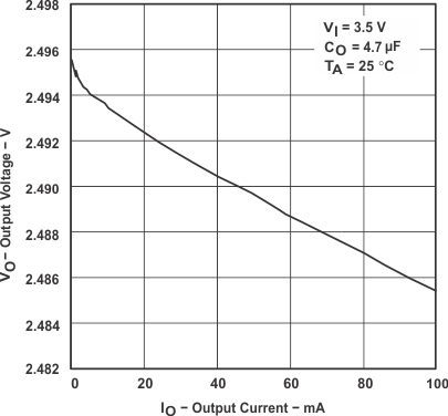
TPS769-Q1 TPS76925-Q1 Output Voltage vs Output Current (Legacy Chip)
 
Figure 5-1 TPS76925-Q1 Output Voltage vs Output Current (Legacy Chip)
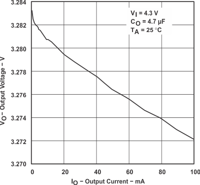
TPS769-Q1 TPS76933-Q1 Output Voltage vs Output Current (Legacy Chip)
 
Figure 5-3 TPS76933-Q1 Output Voltage vs Output Current (Legacy Chip)
TPS769-Q1 TPS76933-Q1 Output Voltage vs Output Current (New Chip)
TJ = 25°C
Figure 5-5 TPS76933-Q1 Output Voltage vs Output Current (New Chip)
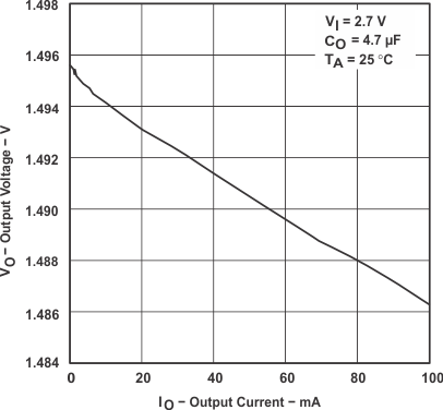
TPS769-Q1 TPS76915-Q1 Output Voltage vs Output Current (Legacy Chip)
 
Figure 5-2 TPS76915-Q1 Output Voltage vs Output Current (Legacy Chip)
TPS769-Q1 TPS76933-Q1 Output Voltage vs Output Current (New Chip)
TJ = 25°C
Figure 5-4 TPS76933-Q1 Output Voltage vs Output Current (New Chip)
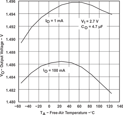
TPS769-Q1 TPS76915-Q1 Output Voltage vs Free-Air Temperature (Legacy Chip)
 
Figure 5-6 TPS76915-Q1 Output Voltage vs Free-Air Temperature (Legacy Chip)
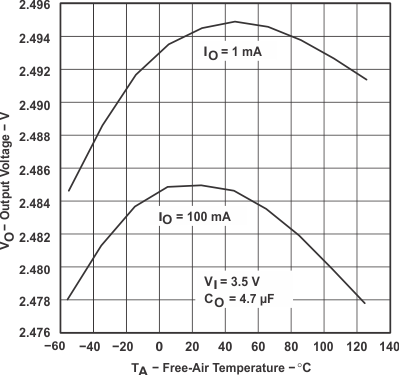
TPS769-Q1 TPS76925-Q1 Output Voltage vs Free-Air Temperature (Legacy Chip)
 
Figure 5-7 TPS76925-Q1 Output Voltage vs Free-Air Temperature (Legacy Chip)
TPS769-Q1 TPS76933-Q1 Output Voltage vs Free-Air Temperature (New Chip)
 
Figure 5-9 TPS76933-Q1 Output Voltage vs Free-Air Temperature (New Chip)
TPS769-Q1 TPS76933-Q1 Load Regulation vs Free-Air Temperature (New Chip)
 
Figure 5-11 TPS76933-Q1 Load Regulation vs Free-Air Temperature (New Chip)
TPS769-Q1 TPS76933-Q1 Ground Current vs Free-Air Temperature (New Chip)
 
Figure 5-13 TPS76933-Q1 Ground Current vs Free-Air Temperature (New Chip)
TPS769-Q1 TPS76933-Q1 Ground Current vs Output Current (New Chip)
 
Figure 5-15 TPS76933-Q1 Ground Current vs Output Current (New Chip)
TPS769-Q1 TPS76933-Q1 Ground Current vs Input Supply (New Chip)
 
Figure 5-17 TPS76933-Q1 Ground Current vs Input Supply (New Chip)
TPS769-Q1 TPS76933-Q1 EN Threshold vs Free-Air Temperature (New Chip)
 
Figure 5-19 TPS76933-Q1 EN Threshold vs Free-Air Temperature (New Chip)
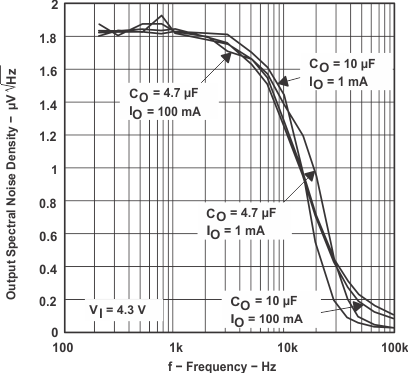
TPS769-Q1 TPS76933-Q1 Output Spectral Noise Density vs Frequency (Legacy
                        Chip)
 
Figure 5-21 TPS76933-Q1 Output Spectral Noise Density vs Frequency (Legacy Chip)
TPS769-Q1 TPS76933-Q1 Output Spectral Noise Density vs Output Capacitor (New
                        Chip)
 
Figure 5-23 TPS76933-Q1 Output Spectral Noise Density vs Output Capacitor (New Chip)
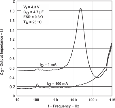
TPS769-Q1 Output Impedance vs Frequency (Legacy Chip)
 
Figure 5-25 Output Impedance vs Frequency (Legacy Chip)
TPS769-Q1 TPS76933-Q1 Dropout Voltage vs Free-Air Temperature (New Chip)
 
Figure 5-27 TPS76933-Q1 Dropout Voltage vs Free-Air Temperature (New Chip)
TPS769-Q1 TPS76901-Q1 Dropout Voltage vs Input Supply (New Chip)
 
Figure 5-29 TPS76901-Q1 Dropout Voltage vs Input Supply (New Chip)
TPS769-Q1 TPS76933-Q1 Ripple Rejection vs Output Current (New Chip)
 
Figure 5-31 TPS76933-Q1 Ripple Rejection vs Output Current (New Chip)
TPS769-Q1 TPS76901-Q1 Ripple Rejection vs Feed-Forward Capacitor (New Chip)
IOUT = 50mA
Figure 5-33 TPS76901-Q1 Ripple Rejection vs Feed-Forward Capacitor (New Chip)
TPS769-Q1 LDO
                        Start-Up Time With Input Supply (New Chip)
 
Figure 5-35 LDO Start-Up Time With Input Supply (New Chip)
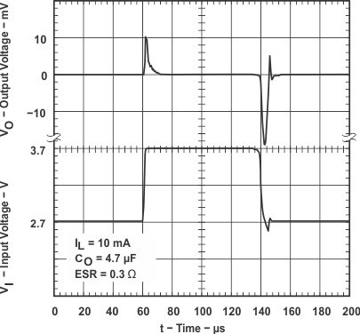
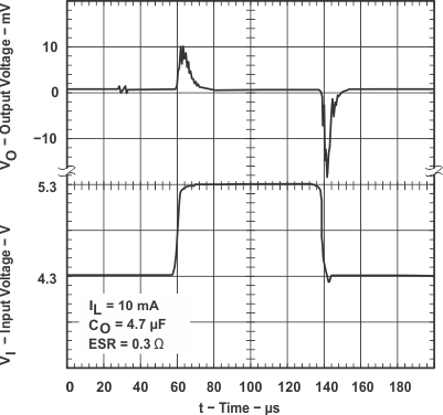
TPS769-Q1 TPS76915-Q1 Line Transient Response (Legacy Chip)
 
Figure 5-37 TPS76915-Q1 Line Transient Response (Legacy Chip)
TPS769-Q1 TPS76933-Q1 Line Transient Response (Legacy Chip)
 
Figure 5-39 TPS76933-Q1 Line Transient Response (Legacy Chip)
TPS769-Q1 TPS76933-Q1 Line Transient Response (New Chip)
4.3V to 16.0V at 1V/μs
Figure 5-41 TPS76933-Q1 Line Transient Response (New Chip)
TPS769-Q1 TPS76933-Q1 Load Transient Response (New Chip)
1mA to 100mA at 1A/μs
Figure 5-43 TPS76933-Q1 Load Transient Response (New Chip)
TPS769-Q1 TPS76933-Q1 Load Transient Response (New Chip)
1mA to 100mA at 1mA/μs
Figure 5-45 TPS76933-Q1 Load Transient Response (New Chip)
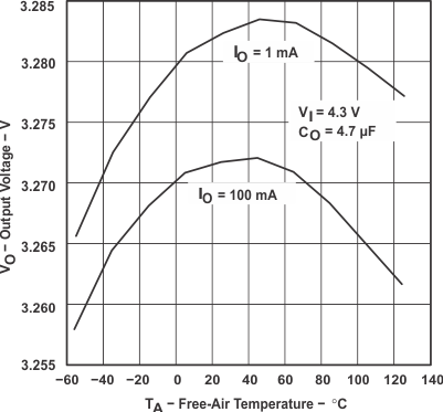
TPS769-Q1 TPS76933-Q1 Output Voltage vs Free-Air Temperature (Legacy Chip)
 
Figure 5-8 TPS76933-Q1 Output Voltage vs Free-Air Temperature (Legacy Chip)
TPS769-Q1 TPS76933-Q1 Line Regulation vs Free-Air Temperature (New Chip)
 
Figure 5-10 TPS76933-Q1 Line Regulation vs Free-Air Temperature (New Chip)
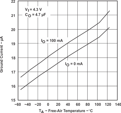
TPS769-Q1 TPS76933-Q1 Ground Current vs Free-Air Temperature (Legacy Chip)
 
Figure 5-12 TPS76933-Q1 Ground Current vs Free-Air Temperature (Legacy Chip)
TPS769-Q1 TPS76933-Q1 Ground Current vs Output Current (New Chip)
TJ = 25°C
Figure 5-14 TPS76933-Q1 Ground Current vs Output Current (New Chip)
TPS769-Q1 TPS76933-Q1 Ground Current vs Input Supply (New Chip)
 
Figure 5-16 TPS76933-Q1 Ground Current vs Input Supply (New Chip)
TPS769-Q1 TPS76933-Q1 UVLO Threshold vs Free-Air Temperature (New Chip)
 
Figure 5-18 TPS76933-Q1 UVLO Threshold vs Free-Air Temperature (New Chip)
TPS769-Q1 TPS76933-Q1 Current Limit vs Free-Air Temperature (New Chip)
 
Figure 5-20 TPS76933-Q1 Current Limit vs Free-Air Temperature (New Chip)
TPS769-Q1 TPS76933-Q1 Output Spectral Noise Density vs Output Current (New
                        Chip)
 
Figure 5-22 TPS76933-Q1 Output Spectral Noise Density vs Output Current (New Chip)
TPS769-Q1 TPS76901-Q1 Output Spectral Noise Density vs Feed-Forward Capacitor (New
                        Chip)
IOUT = 50mA
Figure 5-24 TPS76901-Q1 Output Spectral Noise Density vs Feed-Forward Capacitor (New Chip)
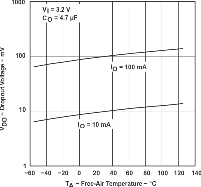
TPS769-Q1 TPS76933-Q1 Dropout Voltage vs Free-Air Temperature (Legacy Chip)
 
Figure 5-26 TPS76933-Q1 Dropout Voltage vs Free-Air Temperature (Legacy Chip)
TPS769-Q1 TPS76933-Q1 Dropout Voltage vs Output Current (New Chip)
 
Figure 5-28 TPS76933-Q1 Dropout Voltage vs Output Current (New Chip)
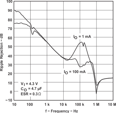
TPS769-Q1 TPS76933-Q1 Ripple Rejection vs Frequency (Legacy Chip)
 
Figure 5-30 TPS76933-Q1 Ripple Rejection vs Frequency (Legacy Chip)
TPS769-Q1 TPS76933-Q1 Ripple Rejection vs Output Capacitor (New Chip)
IOUT = 100mA
Figure 5-32 TPS76933-Q1 Ripple Rejection vs Output Capacitor (New Chip)
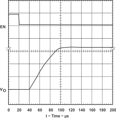
TPS769-Q1 LDO
                        Start-Up Time (Legacy Chip)
 
Figure 5-34 LDO Start-Up Time (Legacy Chip)
TPS769-Q1 LDO
                        Start-Up Time With EN (New Chip)
 
Figure 5-36 LDO Start-Up Time With EN (New Chip)
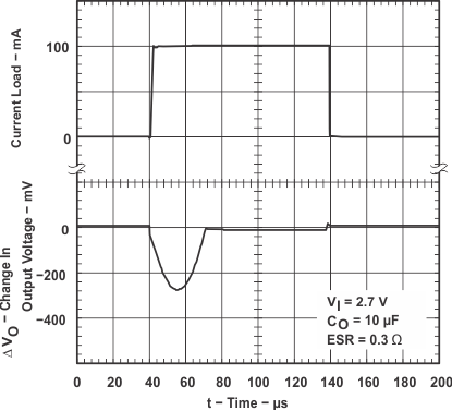
TPS769-Q1 TPS76915-Q1 Load Transient Response (Legacy Chip)
 
Figure 5-38 TPS76915-Q1 Load Transient Response (Legacy Chip)
TPS769-Q1 TPS76933-Q1 Line Transient Response (New Chip)
4.3V to 5.3V at 1V/μs
Figure 5-40 TPS76933-Q1 Line Transient Response (New Chip)
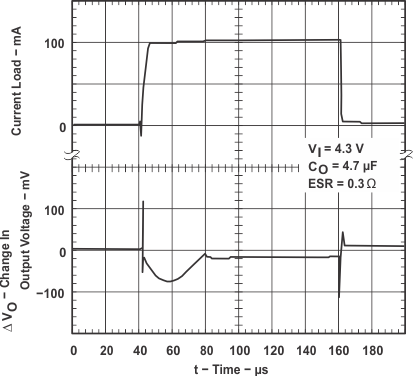
TPS769-Q1 TPS76933-Q1 Load Transient Response (Legacy Chip)
 
Figure 5-42 TPS76933-Q1 Load Transient Response (Legacy Chip)
TPS769-Q1 TPS76933-Q1 Load Transient Response (New Chip)
1μA to 100mA at 1A/μs
Figure 5-44 TPS76933-Q1 Load Transient Response (New Chip)