SBVS411A August 2020 – October 2020 TPS784
PRODUCTION DATA
- 1 Features
- 2 Applications
- 3 Description
- 4 Revision History
- 5 Pin Configuration and Functions
- 6 Specifications
- 7 Detailed Description
-
8 Application and Implementation
- 8.1 Application Information
- 8.2 Typical Application
- 9 Power Supply Recommendations
- 10Layout
- 11Device and Documentation Support
- 12Mechanical, Packaging, and Orderable Information
Package Options
Mechanical Data (Package|Pins)
- DBV|5
Thermal pad, mechanical data (Package|Pins)
Orderable Information
7.3.4 Undervoltage Lockout (UVLO) Operation
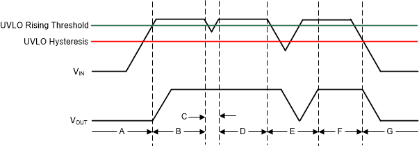
The UVLO circuit ensures that the device stays disabled before its input supply reaches the minimum operational voltage range, and ensures that the device shuts down when the input supply collapses. Figure 7-2 shows the UVLO circuit response to various input voltage events. The diagram can be separated into the following parts:
- Region A: The device does not start until the input reaches the UVLO rising threshold.
- Region B: Normal operation, regulating device.
- Region C: Brownout event above the UVLO falling threshold (UVLO rising threshold – UVLO hysteresis). The output may fall out of regulation but the device remains enabled.
- Region D: Normal operation, regulating device.
- Region E: Brownout event below the UVLO falling threshold. The device is disabled in most cases and the output falls because of the load and active discharge circuit. The device is reenabled when the UVLO rising threshold is reached by the input voltage and a normal start-up follows.
- Region F: Normal operation followed by the input falling to the UVLO falling threshold.
- Region G: The device is disabled when the input voltage falls below the UVLO falling threshold to 0 V. The output falls because of the load and active discharge circuit.
 Figure 7-2 Typical UVLO
Operation