SBVS097G march 2008 – june 2023 TPS799-Q1
PRODUCTION DATA
- 1
- 1 Features
- 2 Applications
- 3 Description
- 4 Revision History
- 5 Pin Configuration and Functions
- 6 Specifications
- 7 Detailed Description
- 8 Application and Implementation
- 9 Device and Documentation Support
- 10Mechanical, Packaging, and Orderable Information
Package Options
Mechanical Data (Package|Pins)
Thermal pad, mechanical data (Package|Pins)
- DRV|6
Orderable Information
5 Pin Configuration and Functions
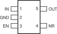
 Figure 5-1 DDC Package,5-Pin SOT-23(Top View)
 Figure 5-2 DRV Package,6-Pin WSON(Top View)
Table 5-1 Pin Functions
| PIN | TYPE | DESCRIPTION | ||
|---|---|---|---|---|
| NAME | SOT-23 | WSON | ||
| EN | 3 | 4 | I | Driving the enable pin (EN) high turns on the regulator. Driving this pin low puts the regulator into shutdown mode. EN can be connected to IN if not used. |
| FB | — | 2 | I | Adjustable version only; this pin is the input to the control loop error amplifier, and is used to set the output voltage of the device. |
| GND | 2 | 3, Pad | — | Ground. The pad must be tied to GND. |
| IN | 1 | 6 | I | Input supply. |
| N/C | — | 5 | — | Not internally connected. This pin must either be left open or tied to GND. |
| NR | 4 | 2 | — | Fixed-voltage versions only; connecting an external capacitor to this pin bypasses noise generated by the internal band gap. This capacitor allows output noise to be reduced to very low levels. |
| OUT | 5 | 1 | O | Output of the regulator. A small capacitor (total typical capacitance ≥ 2 μF ceramic) is needed from this pin to ground to ensure stability. |