TPS799Lxx 200-mA, Low-Dropout Linear Regulator with Built-In Inrush Current Protection
1 Features
- 200-mA Low-Dropout Regulator with EN
- Multiple Output Voltage Versions Available:
- TPS799L: Fixed Outputs of 5.2 V to 6.2 V Using Innovative Factory EEPROM Programming
- TPS799L57: 5.7-V Output
- TPS799L54: 5.4-V Output
- TPS799: Output Options Less Than 5.2 V
- Inrush current Protection with EN Toggle
- Low IQ: 40 μA
- High PSRR: 66 dB at 1 kHz
- Stable with a Low-ESR, 2.0-μF Typical Output Capacitance
- Excellent Load and Line Transient Response
- 2% Overall Accuracy (Load, Line, and Temperature)
- Very Low Dropout: 100 mV
- Package: 5-Bump, Thin, 1-mm × 1.37-mm DSBGA
2 Applications
- Cellular Phones
- Wireless LAN, Bluetooth®
- VCOs, RF
- Handheld Organizers, PDAs
3 Description
The TPS799L family of low-dropout (LDO), low-power linear regulators offers excellent ac performance with very low ground current. High power-supply rejection ratio (PSRR), low noise, fast start-up, and excellent line and load transient response are provided while consuming a very low 40-μA (typical) ground current.
The TPS799Lxx is stable with ceramic capacitors and uses an advanced BiCMOS fabrication process to yield a dropout voltage of typically 100 mV at a
200-mA output. The TPS799L uses a precision voltage reference and feedback loop to achieve an overall accuracy of 2% over all load, line, process, and temperature variations. The TPS799L features inrush current protection when the EN toggle is used to start the device, immediately clamping the current.
All devices are fully specified over the temperature range of TJ = –40°C to 125°C, and offered in a low-profile, die-sized ball grid array (DSBGA) package, ideal for wireless handsets and WLAN cards.
Device Information(1)
| PART NUMBER | PACKAGE | BODY SIZE (NOM) |
|---|---|---|
| TPS799Lxx | DSBGA (5) | 1.57 mm × 1.20 mm |
- For all available packages, see the package option addendum at the end of the datasheet.
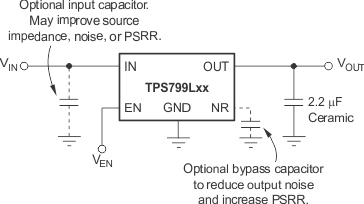
Typical Application Circuit
4 Revision History
Changes from A Revision (July 2012) to B Revision
- Changed document format; added new sections and moved existing sectionsGo
- Added TPS799L54 device to data sheetGo
- Changed WCSP package name to DSBGA throughout data sheetGo
- Changed free-air to junction in Absolute Maximum Ratings table conditionsGo
- Changed free-air to junction in Recommended Operating Conditions table conditionsGo
- Deleted Start-up time symbolGo
Changes from * Revision (April 2012) to A Revision
- Deleted Figure 19Go
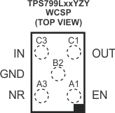
5 Pin Configuration and Functions

Pin Functions
| PIN | I/O | DESCRIPTION | |
|---|---|---|---|
| NAME | NO. | ||
| EN | A1 | I | Driving this pin high turns on the regulator. Driving this pin low puts the regulator into shutdown mode. EN can be connected to IN if not used. |
| GND | B2 | — | Ground |
| IN | C3 | I | Input supply |
| NR | A3 | — | Noise reduction; connecting this pin to an external capacitor bypasses noise generated by the internal band gap. This capacitor allows output noise to be reduced to very low levels. |
| OUT | C1 | O | Output of the regulator. To assure stability, a small ceramic capacitor (total typical capacitance ≥ 2.0 μF) is required from this pin to ground. |
6 Specifications
6.1 Absolute Maximum Ratings
over operating junction temperature range (unless otherwise noted)(1)| MIN | MAX | UNIT | ||
|---|---|---|---|---|
| Voltage(2) | IN | –0.3 | 7.0 | V |
| EN | –0.3 | VIN + 0.3 | V | |
| OUT | –0.3 | VIN + 0.3 | V | |
| Current | OUT | Internally limited | mA | |
| Temperature | Operating virtual junction, TJ | –55 | 150 | °C |
6.2 Handling Ratings
| MIN | MAX | UNIT | |||
|---|---|---|---|---|---|
| Tstg | Storage temperature range | –55 | 150 | °C | |
| V(ESD) | Electrostatic discharge | Human body model (HBM), per ANSI/ESDA/JEDEC JS-001, all pins(1) | –2000 | 2000 | V |
| Charged device model (CDM), per JEDEC specification JESD22-C101, all pins(2) | –500 | 500 | |||
6.3 Recommended Operating Conditions
over operating junction temperature range (unless otherwise noted)| MIN | NOM | MAX | UNIT | ||
|---|---|---|---|---|---|
| VIN | Input voltage | 2.7 | 6.5 | V | |
| IOUT | Output current | 0.5 | 200 | mA | |
| TJ | Operating junction temperature | –40 | 125 | °C | |
6.4 Thermal Information
| THERMAL METRIC(1) | TPS799Lxx | UNIT | |
|---|---|---|---|
| YZY (DSBGA) | |||
| 5 PINS | |||
| RθJA | Junction-to-ambient thermal resistance | 143.3 | °C/W |
| RθJC(top) | Junction-to-case (top) thermal resistance | 1.1 | |
| RθJB | Junction-to-board thermal resistance | 84.7 | |
| ψJT | Junction-to-top characterization parameter | 3.8 | |
| ψJB | Junction-to-board characterization parameter | 84.4 | |
| RθJC(bot) | Junction-to-case (bottom) thermal resistance | N/A | |
6.5 Electrical Characteristics
Over operating temperature range (TJ = –40°C to 125°C), VIN = VOUT(TYP) + 0.3 V or 2.7 V, whichever is greater; IOUT = 1 mA, VEN = VIN, COUT = 2.2 μF, CNR = 0.01 μF, unless otherwise noted. Typical values are at TJ = 25°C.| PARAMETER | TEST CONDITIONS | MIN | TYP | MAX | UNIT | ||
|---|---|---|---|---|---|---|---|
| VIN | Input voltage range(1) | 2.7 | 6.5 | V | |||
| VOUT | Output voltage range | 5.2 | 6.2 | V | |||
| Output accuracy, nominal | TJ = 25°C | –1.0% | 1.0% | ||||
| Output accuracy(1)
Over VIN, IOUT, temperature |
VOUT + 0.3 V ≤ VIN ≤ 6.5 V 500 μA ≤ IOUT ≤ 200 mA |
–2.0% | ±1.0% | 2.0% | |||
| ΔVO(ΔVI) | Line regulation(1) | VOUT(NOM) + 0.3 V ≤ VIN ≤ 6.5 V | 0.02 | %/V | |||
| ΔVO(ΔIO) | Load regulation | 500 μA ≤ IOUT ≤ 200 mA | 0.002 | %/mA | |||
| VDO | Dropout voltage (VIN = VOUT(NOM) – 0.1 V) |
VOUT ≥ 3.3 V, IOUT = 200 mA | 90 | 160 | mV | ||
| ILIM | Output current limit(2) | VOUT = 0.9 × VOUT(NOM) | 220 | 340 | 600 | mA | |
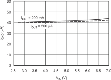
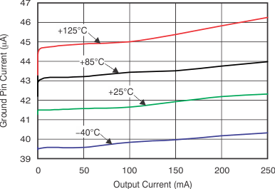
| IGND | Ground pin current | 500 μA ≤ IOUT ≤ 200 mA | 40 | 60 | μA | ||
| ISHDN | Shutdown current (IGND) | VEN ≤ 0.4 V, 2.7 V ≤ VIN ≤ 6.5 V | 0.15 | 1.0 | μA | ||
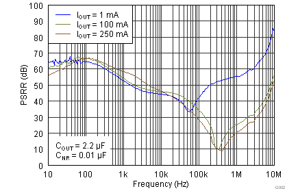
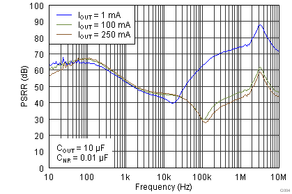
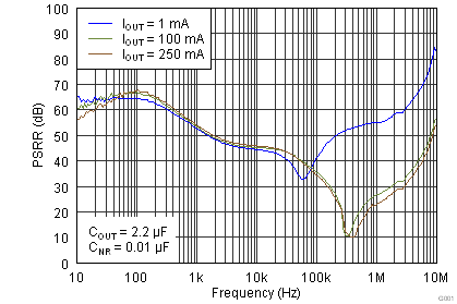
| PSRR | Power-supply rejection ratio | VIN = 6.5 V, VOUT = 2.85 V, CNR = 0.01 μF, IOUT = 100 mA |
f = 100 Hz | 70 | dB | ||
| f = 1 kHz | 66 | dB | |||||
| f = 10 kHz | 51 | dB | |||||
| f = 100 kHz | 38 | dB | |||||
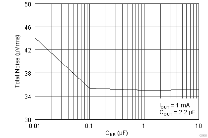
| VN | Output noise voltage | BW = 10 Hz to 100 kHz | CNR = 0.01 μF | 10.5 × VOUT | μVRMS | ||
| CNR = none | 94 × VOUT | μVRMS | |||||
| Start-up time | VOUT = 5.7 V, RL = 28 Ω, COUT = 2.2 μF |
CNR = 0.01 μF | 90 | μs | |||
| CNR = none | 95 | μs | |||||
| VEN(HI) | Enable high (enabled) | 1.2 | VIN | V | |||
| VEN(LO) | Enable low (shutdown) | 0 | 0.4 | V | |||
| IEN(HI) | Enable pin current, enabled | VEN = VIN = 6.5 V | 0.03 | 1.0 | μA | ||
| Tsd | Thermal shutdown temperature | Shutdown, temperature increasing | 165 | °C | |||
| Reset, temperature decreasing | 145 | °C | |||||
| TJ | Operating junction temperature | –40 | 125 | °C | |||
| UVLO | Undervoltage lockout | VIN rising | 1.90 | 2.20 | 2.65 | V | |
| Hysteresis | VIN falling | 70 | mV | ||||
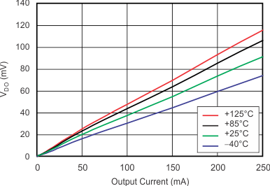
6.6 Typical Characteristics
Over operating temperature range (TJ= –40°C to 125°C), VIN = VOUT(TYP) + 0.3 V or 2.7 V, whichever is greater; IOUT = 1 mA, VEN = VIN, COUT = 2.2 μF, and CNR = 0.01μF, unless otherwise noted. Typical values are at TJ = 25°C.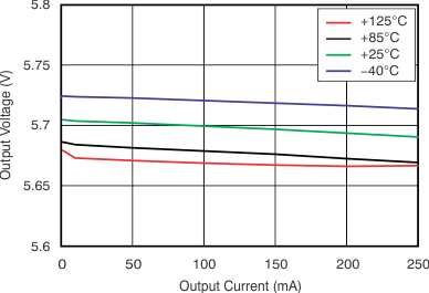
| VIN = 6.5 V |
vs Junction Temperature
| VIN = 6.2 V | ||
| VIN = 6.5 V |
| VIN = 5.95 V |
| VIN = 6 V |
| TPS799Axx | ||
| IOUT = 250 mA |
| VIN = 6.5 V |
| VIN = 6.5 V | ||
| VIN = 5.95 V |
| VIN = 6.2 V |
| VIN = 6 V |

| CIN = COUT = 20 µF | IOUT = 47 mA | |
7 Detailed Description
7.1 Overview
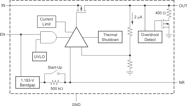
The TPS799Lxx family of low-dropout (LDO) regulators combines the high performance required of many RF and precision analog applications with ultralow current consumption. High PSRR is provided by a high-gain, high-bandwidth error loop with good supply rejection at very low headroom (VIN – VOUT). A noise-reduction pin is provided to bypass noise generated by the band-gap reference and to improve PSRR, while a quick-start circuit quickly charges this capacitor at start-up. The combination of high performance and low ground current also make these devices an excellent choice for portable applications. All versions have thermal and overcurrent protection, and are fully specified from –40°C to 125°C.
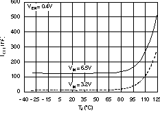
The TPS799Lxx family also features inrush current protection with an EN toggle start-up, and overshoot detection at the output. When the EN toggle is used to start the device, current limit protection is immediately activated, restricting the inrush current to the device (see Figure 16). If voltage at the output overshoots 5% from the nominal value, a pull-down resistor reduces the voltage to normal operating conditions, as shown in the Functional Block Diagram.
7.2 Functional Block Diagram
7.3 Feature Description
7.3.1 Internal Current Limit
The TPS799Lxx internal current limit helps protect the regulator during fault conditions. In current limit mode, the output sources a fixed amount of current that is largely independent of the output voltage. For reliable operation, do not operate the device in a current-limit state for extended periods of time.
The PMOS pass element in the TPS799Lxx has a built-in body diode that conducts current when the voltage at OUT exceeds the voltage at IN. This current is not limited; therefore, if extended reverse voltage operation is anticipated, external limiting may be required.
7.3.2 Shutdown
The enable pin (EN) is active high and is compatible with standard and low-voltage TTL-CMOS levels. When shutdown capability is not required, EN can be connected to IN.
7.3.3 Start Up
The TPS799Lxx uses a start-up circuit to quickly charge the noise reduction capacitor, CNR, if present (see the Functional Block Diagram). This circuit allows for the combination of very low output noise and fast start-up times. The NR pin is high impedance so a low leakage CNR capacitor must be used; most ceramic capacitors are appropriate for this configuration.
Note that for fastest start-up, apply VIN first, and then drive the enable pin (EN) high. If EN is tied to IN, start-up is somewhat slower. The start-up switch is closed for approximately 135 μs. To ensure that CNR is fully charged during start-up, use a 0.01-μF or smaller capacitor.
7.3.4 Undervoltage Lockout (UVLO)
The TPS799Lxx uses an undervoltage lockout circuit to keep the output shut off until internal circuitry is operating properly. The UVLO circuit has a deglitch feature so that undershoot transients are typically ignored on the input if these transients are less than 50 μs in duration.
7.4 Device Functional Modes
Driving EN over 1.2 V turns on the regulator. Driving EN below 0.4 V puts the regulator into shutdown mode, thus reducing the operating current to 150 nA, nominal.
8 Application and Implementation
8.1 Application Information
The TPS799Lxx family of LDO regulators provides high PSRR while maintaining ultralow current consumption. The family also features inrush current protection and overshoot detection at the output.
8.2 Typical Application
Figure 17 shows the basic circuit connections.
Figure 17. Typical Application Circuit
8.2.1 Design Requirements
8.2.1.1 Input and Output Capacitor Requirements
Although an input capacitor is not required for stability, good analog design practice is to connect a 0.1-μF to
1-μF low ESR capacitor across the input supply near the regulator. This capacitor counteracts reactive input sources and improves transient response, noise rejection, and ripple rejection. A higher-value capacitor may be necessary if large, fast rise-time load transients are anticipated, or if the device is located several inches from the power source. If source impedance is not sufficiently low, a 0.1-μF input capacitor may be necessary to ensure stability.
The TPS799Lxx is designed to be stable with standard ceramic capacitors with values of 2.2 μF or greater. X5R- and X7R-type capacitors are best because they have minimal variation in value and ESR over temperature. Maximum ESR must be less than 1.0 Ω.
8.2.1.2 Output Noise
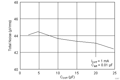
In most LDOs, the band gap is the dominant noise source. If a noise-reduction capacitor (CNR) is used with the TPS799Lxx, the band gap does not contribute significantly to noise. Instead, noise is dominated by the output resistor divider and the error amplifier input. To minimize noise in a given application, use a 0.01-μF noise reduction capacitor. To further optimize noise, equivalent series resistance of the output capacitor can be set to approximately 0.2 Ω. This configuration maximizes phase margin in the control loop, reducing total output noise by up to 10%.
Noise can be referred to the feedback point; with CNR = 0.01 μF total noise is approximately given by Equation 1:

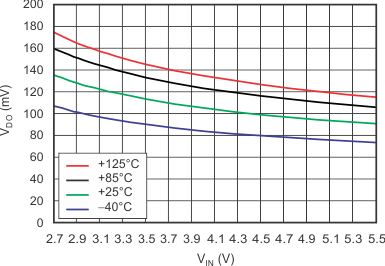
8.2.1.3 Dropout Voltage
The TPS799Lxx uses a PMOS pass transistor to achieve a low dropout voltage. When (VIN – VOUT) is less than the dropout voltage (VDO), the PMOS pass device is in its linear region of operation and rDS(on) of the PMOS pass element is the input-to-output resistance. Because the PMOS device behaves like a resistor in dropout, VDO approximately scales with the output current.
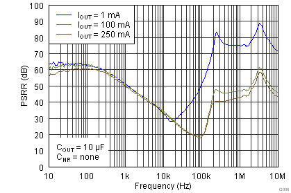
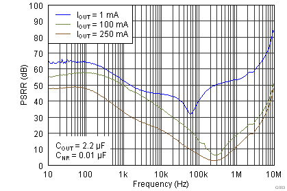
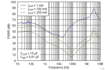
As with any linear regulator, PSRR degrades as (VIN – VOUT) approaches dropout. This effect is illustrated in Figure 8 through Figure 13 in the Typical Characteristics section.
8.2.1.4 Transient Response
As with any regulator, increasing the size of the output capacitor reduces over- and undershoot magnitude, but increases the duration of the transient response. The transient response of the TPS799Lxx is enhanced by an active pull-down device that engages when the output overshoots by approximately 5% or more when the device is enabled. When enabled, the pull-down device behaves like a 350-Ω resistor to ground.
8.2.1.5 Minimum Load
The TPS799Lxx is stable with no output load. To meet the specified accuracy, a minimum load of 500 μA is required. With loads less than 500 μA at junction temperatures near 125°C, the output can drift up enough to cause the output pull-down device to turn on. The output pull-down device limits voltage drift to 5% typically; however, ground current can increase by approximately 50 μA. In typical applications, the junction cannot reach high temperatures at light loads because there is no noticeable dissipated power. The specified ground current is then valid at no load in most applications.
8.2.2 Detailed Design Procedure
Select the desired device based on the output voltage.
Provide an input supply with adequate headroom to account for dropout and output current to account for the GND terminal current, and power the load.
8.2.3 Application Curves
Figure 18. Power-Supply Rejection Ratio vs Frequency
Figure 19. Inrush Current at EN Turn-On
8.3 Do's and Don'ts
Do place at least one 2.2-µF ceramic capacitor as close as possible to the OUT terminal of the regulator.
Do not place the output capacitor more than 10 mm away from the regulator.
Do connect a 0.1-μF to 1.0-μF low equivalent series resistance (ESR) capacitor across the IN terminal and GND input of the regulator.
Do not exceed the absolute maximum ratings.
9 Power-Supply Recommendations
These devices are designed to operate from an input voltage supply range between 2.7 V and 6.5 V. The input voltage range provides adequate headroom in order for the device to have a regulated output. This input supply is well-regulated and stable. If the input supply is noisy, additional input capacitors with low ESR can help improve the output noise performance.
10 Layout
10.1 Layout Guidelines
10.1.1 Board Layout Recommendations to Improve PSRR and Noise Performance
To improve ac performance (such as PSRR, output noise, and transient response), design the board with separate ground planes for VIN and VOUT, with each ground plane connected only at the GND pin of the device. In addition, connect the bypass capacitor directly to the GND pin of the device.
10.1.2 Thermal Information
10.1.2.1 Thermal Protection
Thermal protection disables the output when the junction temperature rises to approximately 165°C, allowing the device to cool. When the junction temperature cools to approximately 145°C the output circuitry is again enabled. Depending on power dissipation, thermal resistance, and ambient temperature, the thermal protection circuit may cycle on and off. This cycling limits the dissipation of the regulator, protecting it from damage resulting from overheating.
Any tendency to activate the thermal protection circuit indicates excessive power dissipation or an inadequate heatsink. For reliable operation, limit junction temperature to 125°C maximum. To estimate the margin of safety in a complete design (including heatsink), increase the ambient temperature until the thermal protection is triggered; use worst-case loads and signal conditions. For good reliability, thermal protection triggers at least 35°C above the maximum expected ambient condition of a particular application. This configuration produces a worst-case junction temperature of 125°C at the highest expected ambient temperature and worst-case load.
The internal protection circuitry of the TPS799Lxx is designed to protect against overload conditions. This circuitry is not intended to replace proper heatsinking. Continuously running the device into thermal shutdown degrades device reliability.
10.1.2.2 Power Dissipation
The ability to remove heat from the die is different for each package type, presenting different considerations in the PCB layout. The PCB area around the device that is free of other components moves the head from the device to the ambient air. Performance data for JEDEC low- and high-K boards are given in the Thermal Information table near the front of this data sheet. Using heavier copper increases the effectiveness in removing heat from the device. The addition of plated through-holes to heat-dissipating layers also improves heatsink effectiveness.
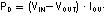
Power dissipation depends on input voltage and load conditions. Power dissipation is equal to the product of the output current times the voltage drop across the output pass element, as shown in Equation 2:
10.1.2.3 Package Mounting
Solder pad footprint recommendations for the TPS799Lxx are available from the Texas Instruments' web site at www.ti.com.
10.2 Layout Example
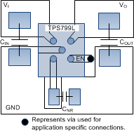 Figure 20. Layout Example
11 Device and Documentation Support
11.1 Device Support
11.1.1 Development Support
11.1.1.1 Evaluation Modules
An evaluation module (EVM) is available to assist in the initial circuit performance evaluation using the TPS799Lxx. This EVM, the TPS799xx evaluation module, can be requested at the Texas Instruments web site through the product folders or purchased directly from the TI eStore.
11.1.1.2 Spice Models
Computer simulation of circuit performance using SPICE is often useful when analyzing the performance of analog circuits and systems. A SPICE model for the TPS799Lxx is available through the product folders under simulation models.
11.1.2 Device Nomenclature
Table 1. Device Nomenclature(1)
| PRODUCT | VOUT |
|---|---|
| TPS799Lxxyyyz | XX is nominal output voltage (for example, 57 = 5.7 V). YYY is package designator. Z is package quantity. |
11.2 Documentation Support
11.2.1 Related Documentation
For related documentation, see the following user guide:
- TPS799XXEVM-105 Evaluation Module, SLVU130
11.3 Related Links
Table 2 lists quick access links. Categories include technical documents, support and community resources, tools and software, and quick access to sample or buy.
Table 2. Related Links
| PARTS | PRODUCT FOLDER | SAMPLE & BUY | TECHNICAL DOCUMENTS | TOOLS & SOFTWARE | SUPPORT & COMMUNITY |
|---|---|---|---|---|---|
| TPS799L54 | Click here | Click here | Click here | Click here | Click here |
| TPS799L57 | Click here | Click here | Click here | Click here | Click here |
11.4 Trademarks
Bluetooth is a registered trademark of Bluetooth SIG, Inc.
All other trademarks are the property of their respective owners.
11.5 Electrostatic Discharge Caution

This integrated circuit can be damaged by ESD. Texas Instruments recommends that all integrated circuits be handled with appropriate precautions. Failure to observe proper handling and installation procedures can cause damage.
ESD damage can range from subtle performance degradation to complete device failure. Precision integrated circuits may be more susceptible to damage because very small parametric changes could cause the device not to meet its published specifications.
11.6 Glossary
SLYZ022 — TI Glossary.
This glossary lists and explains terms, acronyms, and definitions.