SBVS316B September   2018  – December 2020 TPS7A11

PRODUCTION DATA  

  1. Features
  2. Applications
  3. Description
  4. Revision History
  5. Pin Configuration and Functions
  6. Specifications
    1. 6.1 Absolute Maximum Ratings
    2. 6.2 ESD Ratings
    3. 6.3 Recommended Operating Conditions
    4. 6.4 Thermal Information
    5. 6.5 Electrical Characteristics
    6. 6.6 Typical Characteristics
  7. Detailed Description
    1. 7.1 Overview
    2. 7.2 Functional Block Diagram
    3. 7.3 Feature Description
      1. 7.3.1 Excellent Transient Response
        1. 7.3.1.1 Global Undervoltage Lockout (UVLO)
      2. 7.3.2 Active Discharge
      3. 7.3.3 Enable Pin
      4. 7.3.4 Sequencing Requirement
      5. 7.3.5 Internal Foldback Current Limit
      6. 7.3.6 Thermal Shutdown
    4. 7.4 Device Functional Modes
      1. 7.4.1 Normal Mode
      2. 7.4.2 Dropout Mode
      3. 7.4.3 Disable Mode
  8. Application and Implementation
    1. 8.1 Application Information
      1. 8.1.1 Recommended Capacitor Types
      2. 8.1.2 Input and Output Capacitor Requirements
      3. 8.1.3 Load Transient Response
      4. 8.1.4 Dropout Voltage
      5. 8.1.5 Behavior During Transition From Dropout Into Regulation
      6. 8.1.6 Undervoltage Lockout Circuit Operation
      7. 8.1.7 Power Dissipation (PD)
      8. 8.1.8 Estimating Junction Temperature
      9. 8.1.9 Recommended Area for Continuous Operation
    2. 8.2 Typical Application
      1. 8.2.1 Design Requirements
      2. 8.2.2 Detailed Design Procedures
      3. 8.2.3 Application Curve
  9. Power Supply Recommendations
  10. 10Layout
    1. 10.1 Layout Guidelines
    2. 10.2 Layout Examples
  11. 11Device and Documentation Support
    1. 11.1 Device Support
      1. 11.1.1 Development Support
        1. 11.1.1.1 Evaluation Module
      2. 11.1.2 Spice Model
      3. 11.1.3 Device Nomenclature
    2. 11.2 Documentation Support
      1. 11.2.1 Related Documentation
    3. 11.3 Receiving Notification of Documentation Updates
    4. 11.4 Support Resources
    5. 11.5 Trademarks
    6. 11.6 Electrostatic Discharge Caution
    7. 11.7 Glossary

Package Options

Mechanical Data (Package|Pins)
Thermal pad, mechanical data (Package|Pins)
Orderable Information

Typical Characteristics

at operating temperature TJ = 25°C, VIN = VOUT(NOM) + 0.5 V, VBIAS = VOUT(NOM) + 1.4 V, IOUT = 1 mA, VEN = VIN, CIN = COUT = 2.2 µF, and CBIAS = 0.1 µF (unless otherwise noted)
GUID-06BEFFB6-770B-421F-97B2-200C97613ED8-low.gif
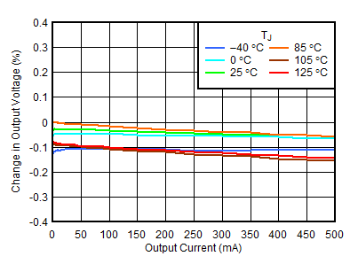
DRV package
Figure 6-1 Output Accuracy vs IOUT and Temperature
GUID-6D37F952-BC7B-4950-B335-1B13EEBA1452-low.gif
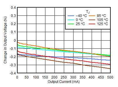
YKA package
Figure 6-3 Output Accuracy vs IOUT and Temperature
GUID-89B65760-F582-410F-9B70-F241AE66590F-low.gif
YKA package
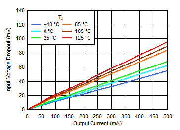
Figure 6-5 VIN Dropout vs IOUT and Temperature
GUID-90ACC43E-2856-43E6-83CB-22CCDFBEE65F-low.gif
 
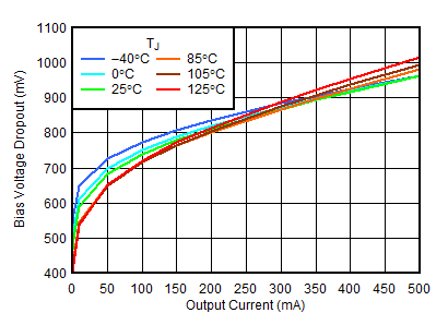
Figure 6-7 VBIAS Dropout vs IOUT and Temperature
GUID-87EE7D9C-438A-4B62-8FBC-9ABF88FBAE7E-low.gif
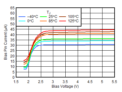
IOUT = 500 mA
Figure 6-9 IQ(BIAS) vs VBIAS and Temperature
GUID-B8F7A596-2723-4C83-8E0E-FE35672795DE-low.gif
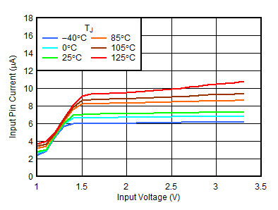
IOUT = 500 mA
Figure 6-11 IQ(IN) vs VIN and Temperature
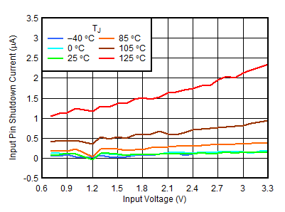
GUID-7984DBF4-CD9D-45C5-9D3A-21AE97F5BA87-low.gif
VOUT = 1.0 V, VEN < 0.4 V
Figure 6-13 ISHDN vs VIN and Temperature
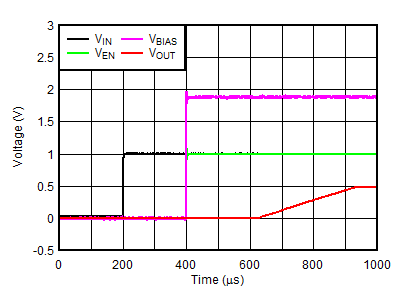
GUID-F376662A-4DE0-443F-A528-6CCC872A8C37-low.gif
VOUT = 0.5 V
Figure 6-15 Startup With VEN and VBIAS Powering Up Simultaneously
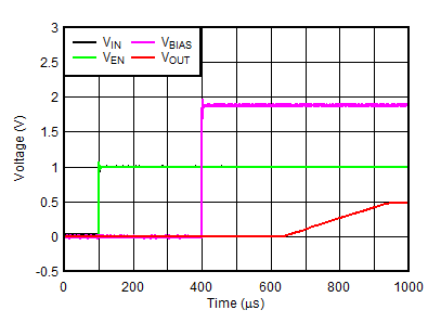
GUID-3DCE2E10-B786-4EC3-B14D-073DD62FF9AF-low.gif
VOUT = 0.5 V
Figure 6-17 Startup With VBIAS Powering Up After VIN and VEN
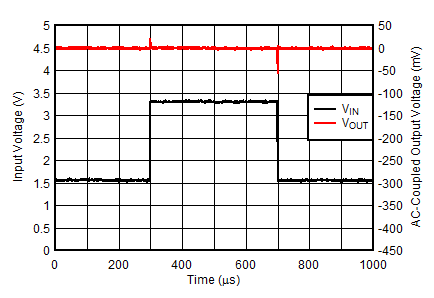
GUID-949A5EDF-C8CF-4403-9A8E-5D3BB009F080-low.gif
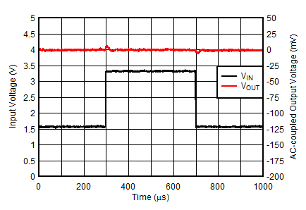
VOUT = 1.0 V, IOUT = 500 mA
Figure 6-19 VIN Transient
GUID-EBB8A9E1-65A2-452E-8ECB-4529DE523377-low.gif
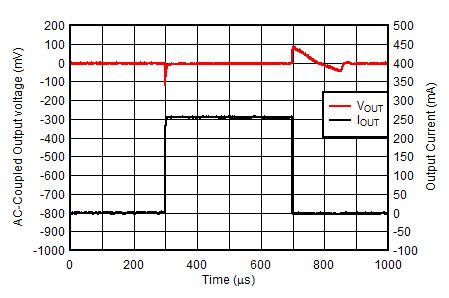
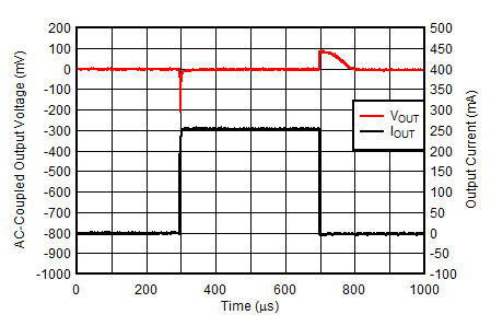
VOUT = 1.0 V, IOUT = 1 mA to 250 mA
Figure 6-21 IOUT Transient
GUID-652A39A7-8096-4F8D-AAEE-F3740211B5C2-low.gif
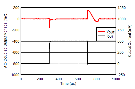
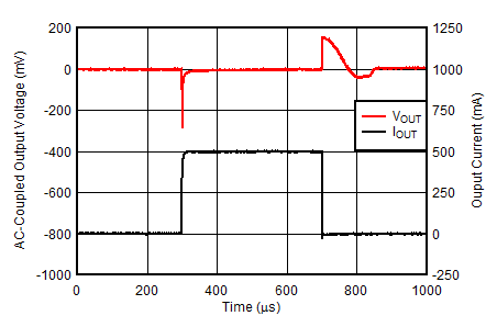
VOUT = 1.0 V, IOUT = 1 mA to 500 mA
Figure 6-23 IOUT Transient
GUID-7246E141-385C-444D-BAF0-DC3A6808A064-low.gif
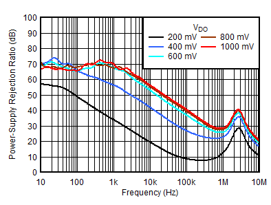
CIN = 0 μF, VOUT = 1.0 V, IOUT = 500 mA, VDO = VIN – VOUT
Figure 6-25 VIN PSRR vs Frequency and Dropout
GUID-E4876A3C-9F29-43AE-B4FC-E4652B8B431C-low.gif
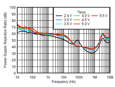
CIN = 2.2 μF, VOUT = 1.0 V, IOUT = 500 mA, CBIAS = 0 μF
Figure 6-27 VBIAS PSRR vs Frequency and VBIAS
GUID-78ADC736-DB6F-4070-8064-9B93ABF80939-low.gif
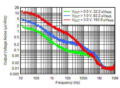
IOUT = 500 mA
Figure 6-29 Output Noise vs Frequency and VOUT
GUID-BBE61ECE-64E1-4CC3-B47A-00159920AA45-low.gif
 
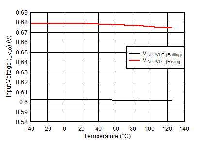
Figure 6-31 VUVLO(IN) Rising and Falling Threshold vs Temperature
GUID-500B93A8-5E4C-4199-9DEA-248E176FF7A3-low.gif
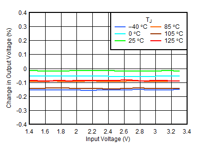
YKA package
Figure 6-2 Output Accuracy vs VIN and Temperature
GUID-92A6CCA0-89EB-4E10-9074-A090A729FF3A-low.gif
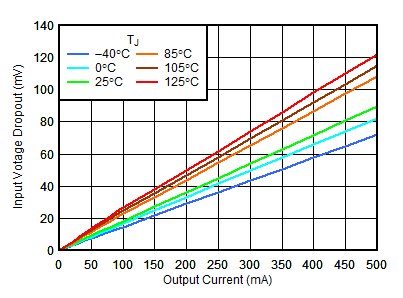
DRV package
Figure 6-4 VIN Dropout vs IOUT and Temperature
GUID-DCED9E7E-EC54-4A5B-A6BC-74A074877CC4-low.gif
 
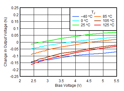
Figure 6-6 Output Accuracy vs VBIAS and Temperature
GUID-354098FD-7F9C-4D72-8554-EBD2DC8C1DB7-low.gif
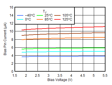
IOUT = 0 mA
Figure 6-8 IQ(BIAS) vs VBIAS and Temperature
GUID-24F88975-5CA6-469C-B3B1-7DE39E868481-low.gif
IOUT = 0 mA
Figure 6-10 IQ(IN) vs VIN and Temperature
GUID-C9EEBE3D-BF1A-4644-953E-F447959EEB1C-low.gif
 
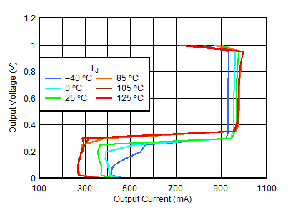
Figure 6-12 Foldback Output Current Limit vs IOUT and Temperature
GUID-067825BD-D186-4B27-AC0E-34AE1EE44346-low.gif
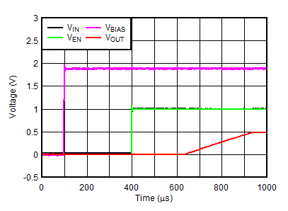
VOUT = 0.5 V
Figure 6-14 Startup With VEN = VIN
GUID-F02D33BF-783B-4EDC-B6F0-89ACCC4877F4-low.gif
VOUT = 0.5 V
Figure 6-16 Startup With Separated VEN
GUID-E0369F58-AEEC-415D-AA7E-94EFA443D33D-low.gif
VOUT = 1.0 V, IOUT = 1 mA
Figure 6-18 VIN Transient
GUID-44F97473-1D64-4B7C-913E-EA230F4AE52B-low.gif
VOUT = 1.0 V, IOUT = 0 mA to 250 mA
Figure 6-20 IOUT Transient
GUID-B6E0C3AD-C2BA-4AEF-8798-9B6B47BF2FAC-low.gif
VOUT = 1.0 V, IOUT = 0 mA to 500 mA
Figure 6-22 IOUT Transient
GUID-69CFFC2A-6DFD-4D65-A9D6-DF534EBFF3BD-low.gif
CIN = 0 μF, VOUT = 1.0 V
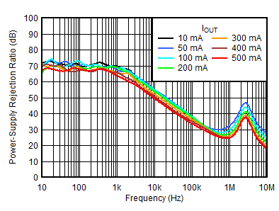
Figure 6-24 VIN PSRR vs Frequency and IOUT
GUID-05D13481-26F6-44FE-A44C-33911C43ECC7-low.gif
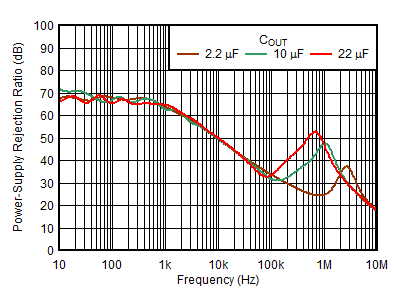
CIN = 0 μF, VOUT = 1.0 V, IOUT = 500 mA
Figure 6-26 VIN PSRR vs Frequency and COUT
GUID-C5254203-8316-4A97-83A8-5C2B6C24A409-low.gif
VOUT = 1.0 V
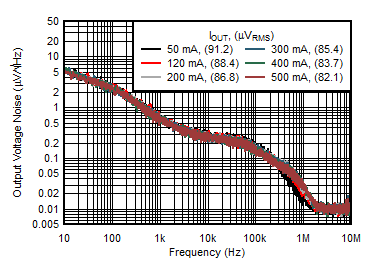
Figure 6-28 Output Noise vs Frequency and IOUT
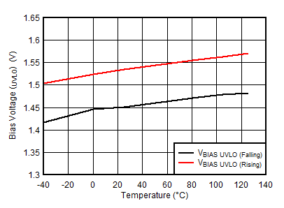
GUID-82A33F5D-9951-41FE-BA49-EA7B4FACE5EF-low.gif
 
Figure 6-30 VUVLO(BIAS) Rising and Falling Threshold vs Temperature
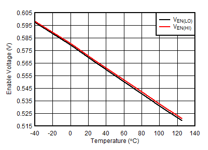
GUID-40AE53E5-71BC-40C4-9BC6-1B2138211051-low.gif
 
Figure 6-32 Enable High and Low Threshold vs Temperature