SBVS400D december   2021  – august 2023 TPS7A14

PRODUCTION DATA  

  1.   1
  2. 1Features
  3. 2Applications
  4. 3Description
  5. 4Revision History
  6. 5Pin Configuration and Functions
  7. 6Specifications
    1. 6.1 Absolute Maximum Ratings
    2. 6.2 ESD Ratings
    3. 6.3 Recommended Operating Conditions
    4. 6.4 Thermal Information
    5. 6.5 Electrical Characteristics
    6. 6.6 Switching Characteristics
    7. 6.7 Typical Characteristics
  8. 7Detailed Description
    1. 7.1 Overview
    2. 7.2 Functional Block Diagram
    3. 7.3 Feature Description
      1. 7.3.1 Excellent Transient Response
      2. 7.3.2 Global Undervoltage Lockout (UVLO)
      3. 7.3.3 Enable Input
      4. 7.3.4 Internal Foldback Current Limit
      5. 7.3.5 Active Discharge
      6. 7.3.6 Thermal Shutdown
    4. 7.4 Device Functional Modes
      1. 7.4.1 Normal Operation
      2. 7.4.2 Dropout Operation
      3. 7.4.3 Disable Mode
  9. 8Application and Implementation
    1. 8.1 Application Information
      1. 8.1.1  Recommended Capacitor Types
      2. 8.1.2  Input, Output, and Bias Capacitor Requirements
      3. 8.1.3  Dropout Voltage
      4. 8.1.4  Behavior During Transition From Dropout Into Regulation
      5. 8.1.5  Device Enable Sequencing Requirement
      6. 8.1.6  Load Transient Response
      7. 8.1.7  Undervoltage Lockout Circuit Operation
      8. 8.1.8  Power Dissipation (PD)
      9. 8.1.9  Estimating Junction Temperature
      10. 8.1.10 Recommended Area for Continuous Operation
    2. 8.2 Typical Application
      1. 8.2.1 Design Requirements
      2. 8.2.2 Detailed Design Procedure
      3. 8.2.3 Application Curve
    3. 8.3 Power Supply Recommendations
    4. 8.4 Layout
      1. 8.4.1 Layout Guidelines
      2. 8.4.2 Layout Examples
  10. 9Device and Documentation Support
    1. 9.1 Device Support
      1. 9.1.1 Development Support
        1. 9.1.1.1 Evaluation Module
      2. 9.1.2 Device Nomenclature
    2. 9.2 Documentation Support
      1. 9.2.1 Related Documentation
    3. 9.3 Receiving Notification of Documentation Updates
    4. 9.4 Support Resources
    5. 9.5 Trademarks
    6. 9.6 Electrostatic Discharge Caution
    7. 9.7 Glossary
  11.   Mechanical, Packaging, and Orderable Information
    1. 10.1 Mechanical Data

Package Options

Mechanical Data (Package|Pins)
Thermal pad, mechanical data (Package|Pins)
Orderable Information

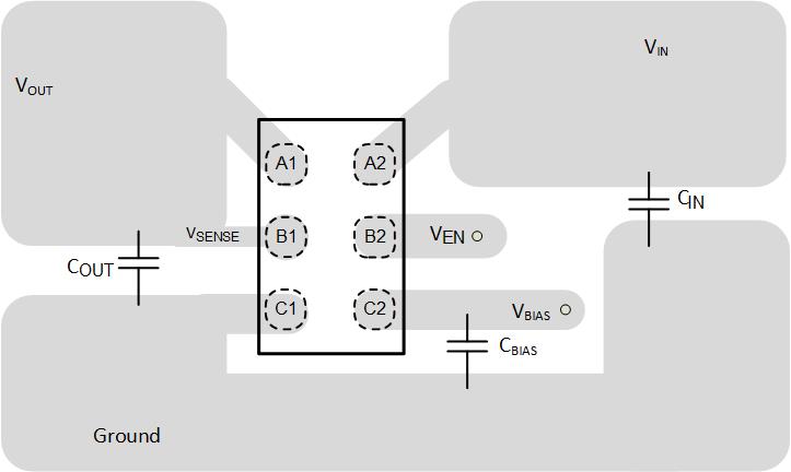
Layout Examples

GUID-20211111-SS0I-JLWT-HGLP-TXJSNVRFGRM7-low.jpgFigure 8-6 Recommended Layout (YBK Package)
GUID-20230816-SS0I-PW1D-57DM-9VWHPLTWPSFK-low.svg Figure 8-7 Recommended Layout (DRV Package)