SBVS400D december 2021 – august 2023 TPS7A14
PRODUCTION DATA
- 1
- 1Features
- 2Applications
- 3Description
- 4Revision History
- 5Pin Configuration and Functions
- 6Specifications
- 7Detailed Description
-
8Application and Implementation
- 8.1
Application Information
- 8.1.1 Recommended Capacitor Types
- 8.1.2 Input, Output, and Bias Capacitor Requirements
- 8.1.3 Dropout Voltage
- 8.1.4 Behavior During Transition From Dropout Into Regulation
- 8.1.5 Device Enable Sequencing Requirement
- 8.1.6 Load Transient Response
- 8.1.7 Undervoltage Lockout Circuit Operation
- 8.1.8 Power Dissipation (PD)
- 8.1.9 Estimating Junction Temperature
- 8.1.10 Recommended Area for Continuous Operation
- 8.2 Typical Application
- 8.3 Power Supply Recommendations
- 8.4 Layout
- 8.1
Application Information
- 9Device and Documentation Support
- Mechanical, Packaging, and Orderable Information
Package Options
Mechanical Data (Package|Pins)
- DRV|6
- YBK|6
Thermal pad, mechanical data (Package|Pins)
- DRV|6
Orderable Information
3 Description
The TPS7A14 is a small, ultra low-dropout regulator (LDO) with excellent transient response. This device can source 1 A with outstanding ac performance (load and line transient responses). The input voltage range is 0.7 V to 2.2 V, and the output range is 0.5 V to 2.0 V with a very high accuracy of 1% over load, line, and temperature.
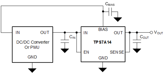
The primary power path is through the IN pin and can be connected to a power supply as low as 50 mV above the output voltage. All electrical characteristics (including excellent output voltage tolerance, transient response, and PSRR) are specified for input voltages 100 mV greater than the output voltage, thereby yielding high practical efficiency. This regulator supports very low input voltages with the use of a higher, externally supplied VBIAS rail that is used to power the internal circuitry of the LDO. For example, the supply voltage to the IN pin can be the output of a high-efficiency, DC/DC step-down regulator and the BIAS pin supply voltage can be a rechargeable battery.
The TPS7A14 is equipped with an active pulldown circuit to quickly discharge the output when disabled, and provides a known start-up state.
The TPS7A14 is available in a 2-mm × 2-mm, 6-pin WSON package and an ultra-small 0.71-mm × 1.16-mm, 6-bump WCSP package.
| PART NUMBER | PACKAGE(1) | PACKAGE SIZE(2) |
|---|---|---|
| TPS7A14 | YBK (WCSP, 6) | 1.16 mm × 0.71 mm |
| DRV (WSON, 6) | 2 mm × 2 mm |
 Typical Application Circuit