SBVS188E march   2012  – may 2023 TPS7A16-Q1

PRODUCTION DATA  

  1.   1
  2. Features
  3. Applications
  4. Description
  5. Revision History
  6. Pin Configuration and Functions
  7. Specifications
    1. 6.1 Absolute Maximum Ratings
    2. 6.2 ESD Ratings
    3. 6.3 Recommended Operating Conditions
    4. 6.4 Thermal Information
    5. 6.5 Electrical Characteristics
    6. 6.6 Typical Characteristics
  8. Detailed Description
    1. 7.1 Overview
    2. 7.2 Functional Block Diagram
    3. 7.3 Feature Description
      1. 7.3.1 Enable (EN)
      2. 7.3.2 Regulated Output (VOUT)
      3. 7.3.3 PG Delay Timer (DELAY)
    4. 7.4 Device Functional Modes
      1. 7.4.1 Power-Good
      2. 7.4.2 Power-Good Delay and Delay Capacitor
  9. Application and Implementation
    1. 8.1 Application Information
    2. 8.2 Typical Applications
      1. 8.2.1 TPS7A1601-Q1 Circuit as an Adjustable Regulator
        1. 8.2.1.1 Design Requirements
        2. 8.2.1.2 Detailed Design Procedure
          1. 8.2.1.2.1 Adjustable Voltage Operation
          2. 8.2.1.2.2 Resistor Selection
          3. 8.2.1.2.3 Capacitor Recommendations
          4. 8.2.1.2.4 Input and Output Capacitor Requirements
          5. 8.2.1.2.5 Feed-Forward Capacitor (Only for Adjustable Version)
          6. 8.2.1.2.6 Transient Response
        3. 8.2.1.3 Application Curves
      2. 8.2.2 Automotive Applications
        1. 8.2.2.1 Design Requirements
        2. 8.2.2.2 Detailed Design Procedure
          1. 8.2.2.2.1 Device Recommendations
        3. 8.2.2.3 Application Curves
      3. 8.2.3 Multicell Battery Packs
        1. 8.2.3.1 Design Requirements
        2. 8.2.3.2 Detailed Design Procedure
        3. 8.2.3.3 Application Curves
      4. 8.2.4 Battery-Operated Power Tools
        1. 8.2.4.1 Design Requirements
        2. 8.2.4.2 Detailed Design Procedure
        3. 8.2.4.3 Application Curves
    3. 8.3 Power Supply Recommendations
    4. 8.4 Layout
      1. 8.4.1 Layout Guidelines
        1. 8.4.1.1 Additional Layout Considerations
        2. 8.4.1.2 Power Dissipation
        3. 8.4.1.3 Thermal Considerations
      2. 8.4.2 Layout Examples
  10. Device and Documentation Support
    1. 9.1 Receiving Notification of Documentation Updates
    2. 9.2 Support Resources
    3. 9.3 Trademarks
    4. 9.4 Electrostatic Discharge Caution
    5. 9.5 Glossary
  11. 10Mechanical, Packaging, and Orderable Information

Package Options

Mechanical Data (Package|Pins)
Thermal pad, mechanical data (Package|Pins)
Orderable Information

Description

The TPS7A16-Q1 ultra-low-power, low-dropout (LDO) voltage regulator offers the benefits of ultra-low quiescent current, high input voltage, and miniaturized, high-thermal-performance packaging.

The TPS7A16-Q1 is designed for continuous or sporadic (power backup) battery-powered applications where ultra-low quiescent current is critical to extending system battery life.

The TPS7A16-Q1 offers an enable pin (EN) compatible with standard CMOS logic and an integrated open-drain, active-high, power-good output (PG) with a user-programmable delay. These pins are intended for use in microcontroller-based, battery-powered applications where power-rail sequencing is required.

In addition, the TPS7A16-Q1 is designed for generating a low-voltage supply from multicell solutions ranging from high-cell-count, power-tool packs to automotive applications; not only can this device supply a well-regulated voltage rail, but the TPS7A16-Q1 can also withstand and maintain regulation during voltage transients. These features translate to simpler and more cost-effective, electrical surge-protection circuitry.

Package Information
PART NUMBER PACKAGE(1) BODY SIZE (NOM)
TPS7A16-Q1 DGN (HVSSOP, 8) 3.00 mm × 3.00 mm
For all available packages, see the orderable addendum at the end of the data sheet.
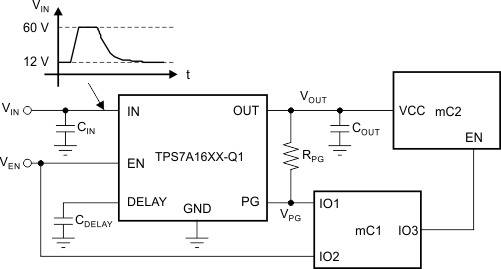
GUID-D000D8E1-89EE-41D6-873B-A141DBBED44A-low.gif Typical Application Schematic