SBVS171F December 2011 – October 2015 TPS7A16
PRODUCTION DATA.
- 1 Features
- 2 Applications
- 3 Description
- 4 Revision History
- 5 Pin Configuration and Functions
- 6 Specifications
- 7 Detailed Description
- 8 Application and Implementation
- 9 Power Supply Recommendations
- 10Layout
- 11Device and Documentation Support
- 12Mechanical, Packaging, and Orderable Information
Package Options
Mechanical Data (Package|Pins)
Thermal pad, mechanical data (Package|Pins)
Orderable Information
8 Application and Implementation
NOTE
Information in the following applications sections is not part of the TI component specification, and TI does not warrant its accuracy or completeness. TI’s customers are responsible for determining suitability of components for their purposes. Customers should validate and test their design implementation to confirm system functionality.
8.1 Application Information
The TPS7A16 family of ultralow power voltage regulators offers the benefit of ultralow quiescent current, high input voltage, and miniaturized, high thermal-performance packaging.
The TPS7A16 family is designed for continuous or sporadic (power backup) battery-operated applications where ultralow quiescent current is critical to extending system battery life.
8.2 Typical Applications
8.2.1 TPS7A1601 Circuit as an Adjustable Regulator
 Figure 14. TPS7A1601 Circuit as an Adjustable Regulator Schematic
8.2.1.1 Design Requirements
Table 2 lists the design parameters.
Table 2. Design Parameters
| DESIGN PARAMETER | EXAMPLE VALUE | |||
|---|---|---|---|---|
| Input voltage range | 5.5 V to 40 V | |||
| Output voltage | 5 V | |||
| Output current rating | 100 mA | |||
| Output capacitor range | 2.2 μF to 100 μF | |||
| Delay capacitor range | 100 pF to 100 nF | |||
8.2.1.2 Detailed Design Procedure
8.2.1.2.1 Adjustable Voltage Operation
The TPS7A1601 has an output voltage range from 1.194 V to 20 V. The nominal output of the device is set by two external resistors, as shown in Figure 15:
 Figure 15. Adjustable Operation
R1 and R2 can be calculated for any output voltage range using the formula shown in Equation 1:

8.2.1.2.1.1 Resistor Selection
TI recommends using resistors in the order of MΩ to keep the overall quiescent current of the system as low as possible (by making the current used by the resistor divider negligible compared to the device’s quiescent current).
If greater voltage accuracy is required, consider the voltage offset contributions as a result of feedback current and use of 0.1% tolerance resistors.
Table 3 shows the resistor combination to achieve a few of the most common rails using commercially available 0.1% tolerance resistors to maximize nominal voltage accuracy, while abiding to the formula shown in Equation 1.
Table 3. Selected Resistor Combinations
| VOUT | R1 | R2 | VOUT/(R1 + R2) « IQ | NOMINAL ACCURACY |
|---|---|---|---|---|
| 1.194 V | 0 Ω | ∞ | 0 µA | ±2% |
| 1.8 V | 1.18 MΩ | 2.32 MΩ | 514 nA | ±(2% + 0.14%) |
| 2..5 V | 1.5 MΩ | 1.37 MΩ | 871 nA | ±(2% + 0.16%) |
| 3.3 V | 2 MΩ | 1.13 MΩ | 1056 nA | ±(2% + 0.35%) |
| 5 V | 3.4 MΩ | 1.07 MΩ | 1115 nA | ±(2% + 0.39%) |
| 10 V | 7.87 MΩ | 1.07 MΩ | 1115 nA | ±(2% + 0.42%) |
| 12 V | 14.3 MΩ | 1.58 MΩ | 755 nA | ±(2% + 0.18%) |
| 15 V | 42.2 MΩ | 3.65 MΩ | 327 nA | ±(2% + 0.19%) |
| 18 V | 16.2 MΩ | 1.15 MΩ | 1038 nA | ±(2% + 0.26%) |
Close attention must be paid to board contamination when using high-value resistors; board contaminants may significantly impact voltage accuracy. If board cleaning measures cannot be ensured, consider using a fixed-voltage version of the TPS7A16 or using resistors in the order of hundreds or tens of kΩ.
8.2.1.2.1.2 Capacitor Recommendations
Low equivalent series resistance (ESR) capacitors should be used for the input, output, and feed-forward capacitors. Ceramic capacitors with X7R and X5R dielectrics are preferred. These dielectrics offer more stable characteristics. Ceramic X7R capacitors offer improved overtemperature performance, while ceramic X5R capacitors are the most cost-effective and are available in higher values.
High ESR capacitors may degrade PSRR.
8.2.1.2.1.3 Input and Output Capacitor Requirements
The TPS7A16 family of ultralow power, high-voltage linear regulators achieves stability with a minimum input capacitance of 0.1 µF and output capacitance of 2.2 µF; however, TI recommends using 10-µF ceramic capacitors to maximize AC performance.
8.2.1.2.1.4 Feed-Forward Capacitor
Although a feed-forward capacitor (CFF) from OUT to FB is not needed to achieve stability, TI recommends using a 0.01-µF feed-forward capacitor to maximize AC performance.
8.2.1.2.1.5 Transient Response
As with any regulator, increasing the size of the output capacitor reduces overshoot and undershoot magnitude but increases the duration of the transient response.
8.2.1.3 Application Curves


8.2.2 Automotive Applications
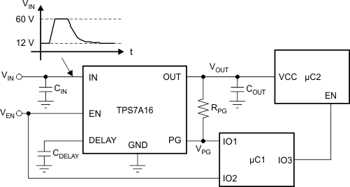
The TPS7A16 family maximum input voltage of 60 V makes it ideal for use in automotive applications where high-voltage transients are present.
Events such as load-dump overvoltage (where the battery is disconnected while the alternator is providing current to a load) may cause voltage spikes from 25 V to 60 V. To prevent any damage to sensitive circuitry, local transient voltage suppressors can be used to cap voltage spikes to lower, more manageable voltages.
The TPS7A16 family can be used to simplify and lower costs in such cases. The TPS7A16 very high voltage range allows this regulator to not only withstand the voltages coming out of these local transient voltage suppressors, but even replace them, thus lowering system cost and complexity.
 Figure 18. Low-Power Microcontroller Rail Sequencing in Automotive Applications Subjected to Load-Dump Transients
8.2.2.1 Design Requirements
Table 4 lists the design parameters.
Table 4. Design Parameters
| DESIGN PARAMETER | EXAMPLE VALUE | |||
|---|---|---|---|---|
| Input voltage range | 5.5 V to 60 V | |||
| Output voltage | 5 V | |||
| Output current rating | 100 mA | |||
| Output capacitor range | 2.2 μF to 100 μF | |||
| Delay capacitor range | 100 pF to 100 nF | |||
8.2.2.2 Detailed Design Procedure
See Capacitor Recommendations and Input and Output Capacitor Requirements.
8.2.2.2.1 Device Recommendations
The output is 5 V, so choose either the fixed output version TPS7A1650 or the adjustable output version TPS7A1601, and set the resistor divider appropriately. See Resistor Selection for more details.
8.2.3 Multicell Battery Packs
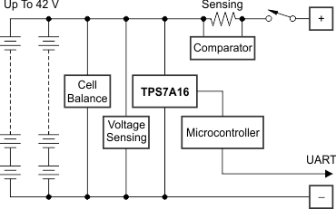
Currently, battery packs can employ up to a dozen cells in series that, when fully charged, may have voltages of up to 55 V. Internal circuitry in these battery packs is used to prevent overcurrent and overvoltage conditions that may degrade battery life or even pose a safety risk; this internal circuitry is often managed by a low-power microcontroller, such as TI’s MSP430.
The microcontroller continuously monitors the battery itself, whether the battery is in use or not. Although this microcontroller could be powered by an intermediate voltage taken from the multicell array, this approach unbalances the battery pack itself, degrading its life or adding cost to implement more complex cell balancing topologies.
The best approach to power this microcontroller is to regulate down the voltage from the entire array to discharge every cell equally and prevent any balancing issues. This approach reduces system complexity and cost.
TPS7A16 is the ideal regulator for this application because it can handle very high voltages (from the entire multicell array) and has very low quiescent current (to maximize battery life).
 Figure 19. Protection Based on Low-Power Microcontroller Power from Multicell Battery Packs
8.2.3.1 Design Requirements
Table 5 lists the design parameters.
Table 5. Device Parameters
| DESIGN PARAMETER | EXAMPLE VALUE | |||
|---|---|---|---|---|
| Input voltage range | 5.5 V to 55 V | |||
| Output voltage | 5 V | |||
| Output current rating | 100 mA | |||
| Output capacitor range | 2.2 μF to 100 μF | |||
| Delay capacitor range | 100 pF to 100 nF | |||
8.2.3.2 Detailed Design Procedure
See Device Recommendations, Capacitor Recommendations, and Input and Output Capacitor Requirements.
8.2.4 Battery-Operated Power Tools
High voltage multicell battery packs support high-power applications, such as power tools, with high current drain when in use, highly intermittent use cycles, and physical separation between battery and motor.
In these applications, a microcontroller or microprocessor controls the motor. This microcontroller must be powered with a low-voltage rail coming from the high-voltage, multicell battery pack; as mentioned previously, powering this microcontroller or microprocessor from an intermediate voltage from the multicell array causes battery-pack life degradation or added system complexity because of cell balancing issues. In addition, this microcontroller or microprocessor must be protected from the high-voltage transients due to the motor inductance.
The TPS7A16 can be used to power the motor-controlled microcontroller or microprocessor; its low quiescent current maximizes battery shelf life and its very high-voltage capabilities simplify system complexity by replacing voltage suppression filters, thus lowering system cost.
 Figure 20. Low Power Microcontroller Power From Multicell Battery Packs In Power Tools
8.2.4.1 Design Requirements
Table 6 lists the design parameters.
Table 6. Design Parameters
| DESIGN PARAMETER | EXAMPLE VALUE | |||
|---|---|---|---|---|
| Input voltage range | 5.5 V to 60 V | |||
| Output voltage | 5 V | |||
| Output current rating | 100 mA | |||
| Output capacitor range | 2.2 μF to 100 μF | |||
| Delay capacitor range | 100 pF to 100 nF | |||
8.2.4.2 Detailed Design Procedure
See Device Recommendations, Capacitor Recommendations, and Input and Output Capacitor Requirements.