SBVS428 May   2022 TPS7A16A

PRODUCTION DATA  

  1. Features
  2. Applications
  3. Description
  4. Revision History
  5. Pin Configuration and Functions
  6. Specifications
    1. 6.1 Absolute Maximum Ratings
    2. 6.2 ESD Ratings
    3. 6.3 Recommended Operating Conditions
    4. 6.4 Thermal Information
    5. 6.5 Electrical Characteristics
    6. 6.6 Typical Characteristics
  7. Detailed Description
    1. 7.1 Overview
    2. 7.2 Functional Block Diagram
    3. 7.3 Feature Description
      1. 7.3.1 Enable (EN)
      2. 7.3.2 Regulated Output (VOUT)
      3. 7.3.3 PG Delay Timer (DELAY)
    4. 7.4 Device Functional Modes
      1. 7.4.1 Power-Good
        1. 7.4.1.1 Power-Good Delay and Delay Capacitor
  8. Application and Implementation
    1. 8.1 Application Information
    2. 8.2 Typical Application
      1. 8.2.1 TPS7A16A Circuit as an Adjustable Regulator
        1. 8.2.1.1 Design Requirements
        2. 8.2.1.2 Detailed Design Procedure
          1. 8.2.1.2.1 Adjustable Voltage Operation
            1. 8.2.1.2.1.1 Resistor Selection
          2. 8.2.1.2.2 Capacitor Recommendations
          3. 8.2.1.2.3 Input and Output Capacitor Requirements
          4. 8.2.1.2.4 Feed-Forward Capacitor (Only for Adjustable Version)
          5. 8.2.1.2.5 Transient Response
        3. 8.2.1.3 Application Curves
  9. Power Supply Recommendations
  10. 10Layout
    1. 10.1 Layout Guidelines
      1. 10.1.1 Additional Layout Considerations
      2. 10.1.2 Power Dissipation
      3. 10.1.3 Thermal Considerations
    2. 10.2 Layout Examples
  11. 11Device and Documentation Support
    1. 11.1 Device Support
      1. 11.1.1 Device Nomenclature
    2. 11.2 Receiving Notification of Documentation Updates
    3. 11.3 Support Resources
    4. 11.4 Trademarks
    5. 11.5 Electrostatic Discharge Caution
    6. 11.6 Glossary
  12. 12Mechanical, Packaging, and Orderable Information
    1. 12.1 Mechanical Data

Package Options

Refer to the PDF data sheet for device specific package drawings

Mechanical Data (Package|Pins)
  • DGN|8
Thermal pad, mechanical data (Package|Pins)
Orderable Information

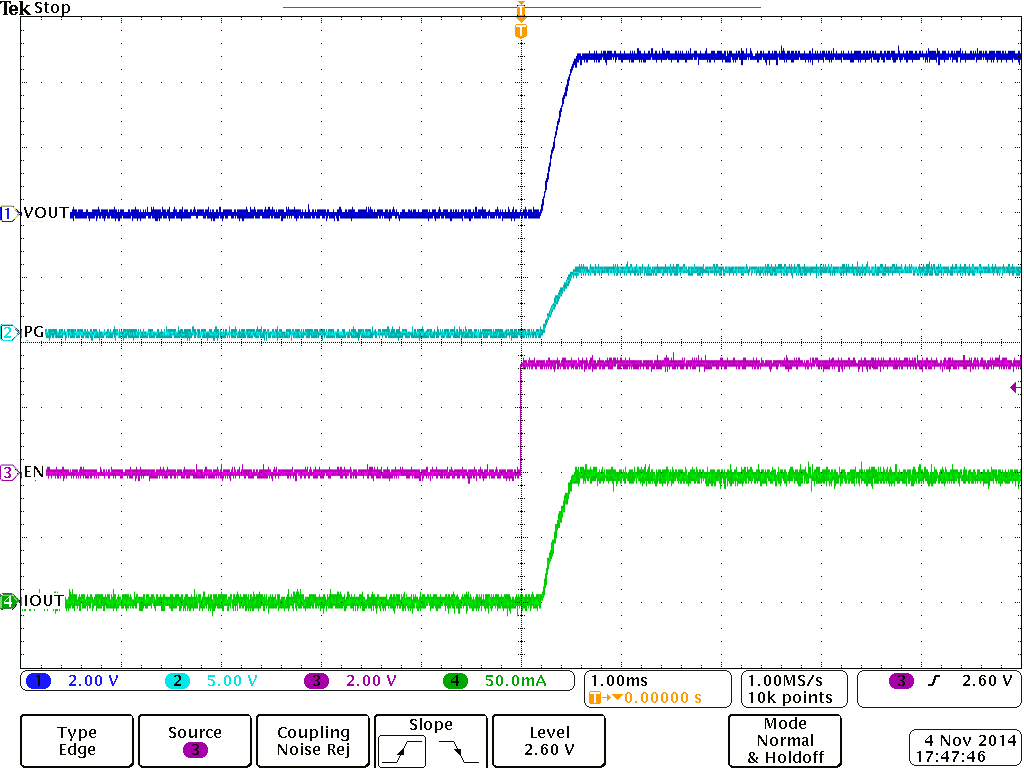
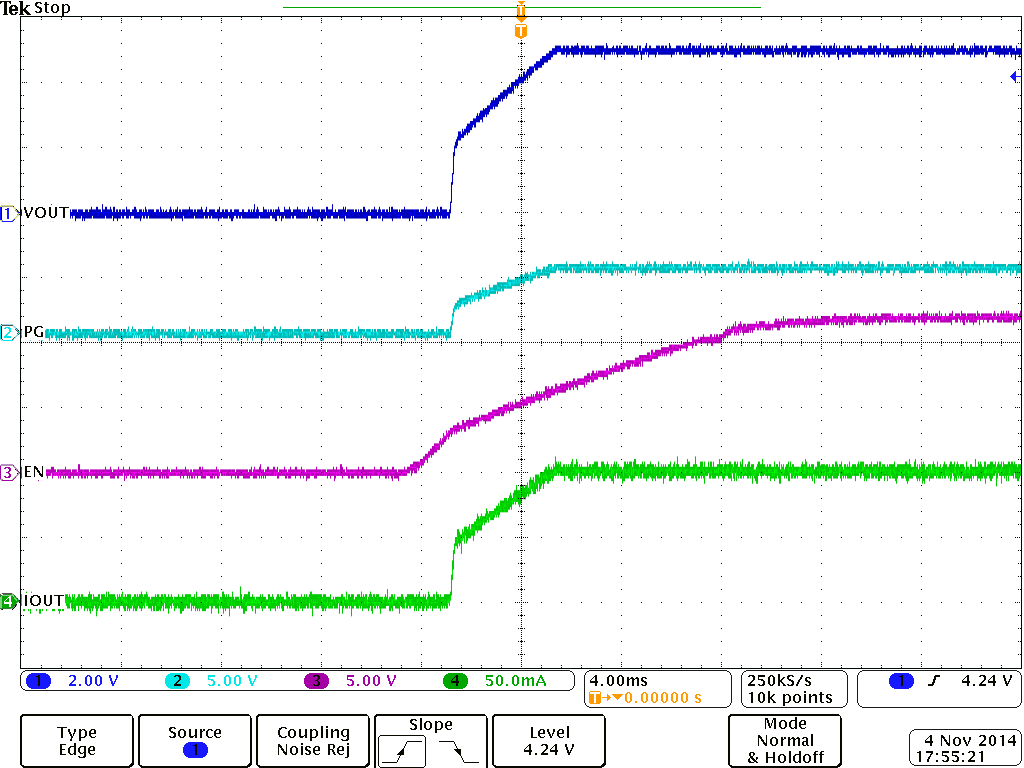
Application Curves

GUID-30CA80F1-EB37-44F7-8510-A28C70FBBD0F-low.png
 
Figure 8-3 Channel 1 is VOUT, Channel 2 is PG, Channel 4 is IOUT, VIN is 12 V and Ready Before EN
GUID-7573FE79-2BC0-426D-ACAF-F0FA4F9F23AF-low.png
 
Figure 8-4 Channel1 is VOUT, Channel 2 is PG, Channel 3 is EN, Channel 4 is IOUT, and VIN is 12 V Connected to EN