SBVS451 August   2024 TPS7A20C

PRODUCTION DATA  

  1.   1
  2. Features
  3. Applications
  4. Description
  5. Pin Configuration and Functions
  6. Specifications
    1. 5.1 Absolute Maximum Ratings
    2. 5.2 ESD Ratings
    3. 5.3 Recommended Operating Conditions
    4. 5.4 Thermal Information
    5. 5.5 Electrical Characteristics
    6. 5.6 Switching Characteristics
    7. 5.7 Typical Characteristics
  7. Detailed Description
    1. 6.1 Overview
    2. 6.2 Functional Block Diagram
    3. 6.3 Feature Description
      1. 6.3.1 Fast Settling
      2. 6.3.2 Low Output Noise
      3. 6.3.3 Dropout Voltage
      4. 6.3.4 Smart Enable
      5. 6.3.5 Current Limit
      6. 6.3.6 Undervoltage Lockout (UVLO)
      7. 6.3.7 Thermal Shutdown
      8. 6.3.8 Active Discharge
    4. 6.4 Device Functional Modes
      1. 6.4.1 Device Functional Mode Comparison
      2. 6.4.2 Normal Operation
      3. 6.4.3 Dropout Operation
      4. 6.4.4 Disabled
  8. Application and Implementation
    1. 7.1 Application Information
      1. 7.1.1 Recommended Capacitor Types
      2. 7.1.2 Input and Output Capacitor Requirements
      3. 7.1.3 Load Transient Response
      4. 7.1.4 Undervoltage Lockout (UVLO) Operation
      5. 7.1.5 Power Dissipation (PD)
        1. 7.1.5.1 Estimating Junction Temperature
        2. 7.1.5.2 Recommended Area for Continuous Operation
    2. 7.2 Typical Application
      1. 7.2.1 Design Requirements
      2. 7.2.2 Detailed Design Procedure
      3. 7.2.3 Application Curve
    3. 7.3 Power Supply Recommendations
    4. 7.4 Layout
      1. 7.4.1 Layout Guidelines
      2. 7.4.2 Layout Example
  9. Device and Documentation Support
    1. 8.1 Device Support
      1. 8.1.1 Device Nomenclature
    2. 8.2 Receiving Notification of Documentation Updates
    3. 8.3 Support Resources
    4. 8.4 Trademarks
    5. 8.5 Electrostatic Discharge Caution
    6. 8.6 Glossary
  10. Revision History
  11. 10Mechanical, Packaging, and Orderable Information
    1. 10.1 Mechanical Data

Package Options

Refer to the PDF data sheet for device specific package drawings

Mechanical Data (Package|Pins)
  • YCK|4
Thermal pad, mechanical data (Package|Pins)
Orderable Information

Typical Characteristics

VIN = VOUT(NOM) + 0.3V or 1.6V (whichever is greater), VOUT = 2.85V, IOUT = 1mA, CIN = 1µF, COUT (derated) = 0.75µF, and TA = 25°C (unless otherwise noted)

TPS7A20C Line Regulation
VEN = 1V
Figure 5-1 Line Regulation
TPS7A20C Dropout Voltage vs IOUT
VEN = 1V
Figure 5-3 Dropout Voltage vs IOUT
TPS7A20C IGND vs IOUT
VEN = 1V (0mA to 300mA)
Figure 5-5 IGND vs IOUT
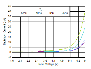
TPS7A20C Shutdown Current vs VIN
VEN = 0V
Figure 5-7 Shutdown Current vs VIN
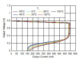
TPS7A20C Current Limit
VEN = 1V
Figure 5-9 Current Limit
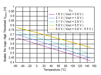
TPS7A20C Enable Logic High Threshold vs Temperature
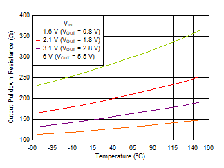
 
Figure 5-11 Enable Logic High Threshold vs Temperature
TPS7A20C Output Pulldown Resistor vs Temperature
VEN = 0.25V
Figure 5-13 Output Pulldown Resistor vs Temperature
TPS7A20C Load Transient
IOUT = 50mA to 200mA, tRISING = 1µs
Figure 5-15 Load Transient
TPS7A20C Load Transient
IOUT = 50mA to 200mA, tRISING = 150ns
Figure 5-17 Load Transient
TPS7A20C Load Transient
IOUT = 1mA to 300mA, tRISING = 1µs
Figure 5-19 Load Transient
TPS7A20C Load Transient
IOUT = 1mA to 300mA, tRISING = 200ns
Figure 5-21 Load Transient
TPS7A20C Load Transient
IOUT = 0mA to 300mA, tRISING = 1µs
Figure 5-23 Load Transient
TPS7A20C Load Transient
IOUT = 0mA to 300mA, tRISING = 200ns
Figure 5-25 Load Transient
TPS7A20C Line Transient
VIN = 3.1V → 4.1V → 3.1V, VIN tRISING = 5µs, IOUT = 150mA
Figure 5-27 Line Transient
TPS7A20C PSRR vs Frequency and IOUT
VIN = 3.15V, VEN = 1V, CIN = 0.47µF
Figure 5-29 PSRR vs Frequency and IOUT
TPS7A20C Noise vs Frequency and IOUT
VRMS BW = 10Hz to 100kHz
Figure 5-31 Noise vs Frequency and IOUT
TPS7A20C Noise vs Frequency and VIN
IOUT = 300mA, VRMS BW = 10Hz to 100kHz
Figure 5-33 Noise vs Frequency and VIN
TPS7A20C Noise vs Frequency and COUT
VIN = 3.85V, IOUT = 300mA, VRMS BW = 10Hz to 100kHz
Figure 5-35 Noise vs Frequency and COUT
TPS7A20C Start-Up
VIN = 0V to 3.85V, VEN = 0V to 3.85V, VEN rises 500µs behind VIN, VIN and VEN slew rate = 1V/µs
Figure 5-37 Start-Up
TPS7A20C Start-Up
VIN = VEN = 0V to 3.85V, VIN and slew rate = 1V/µs
 
Figure 5-39 Start-Up
TPS7A20C Load Regulation
VEN = 1V
Figure 5-2 Load Regulation
TPS7A20C I GND vs VIN
VEN = 1V, IOUT = 0mA
Figure 5-4 I GND vs VIN
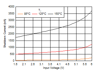
TPS7A20C Shutdown Current vs VIN
VEN = 0V
Figure 5-6 Shutdown Current vs VIN
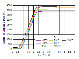
TPS7A20C Enable Pin Leakage Current vs VEN – VIN
VEN = 6V, IOUT = 0mA
Figure 5-8 Enable Pin Leakage Current vs
VEN – VIN
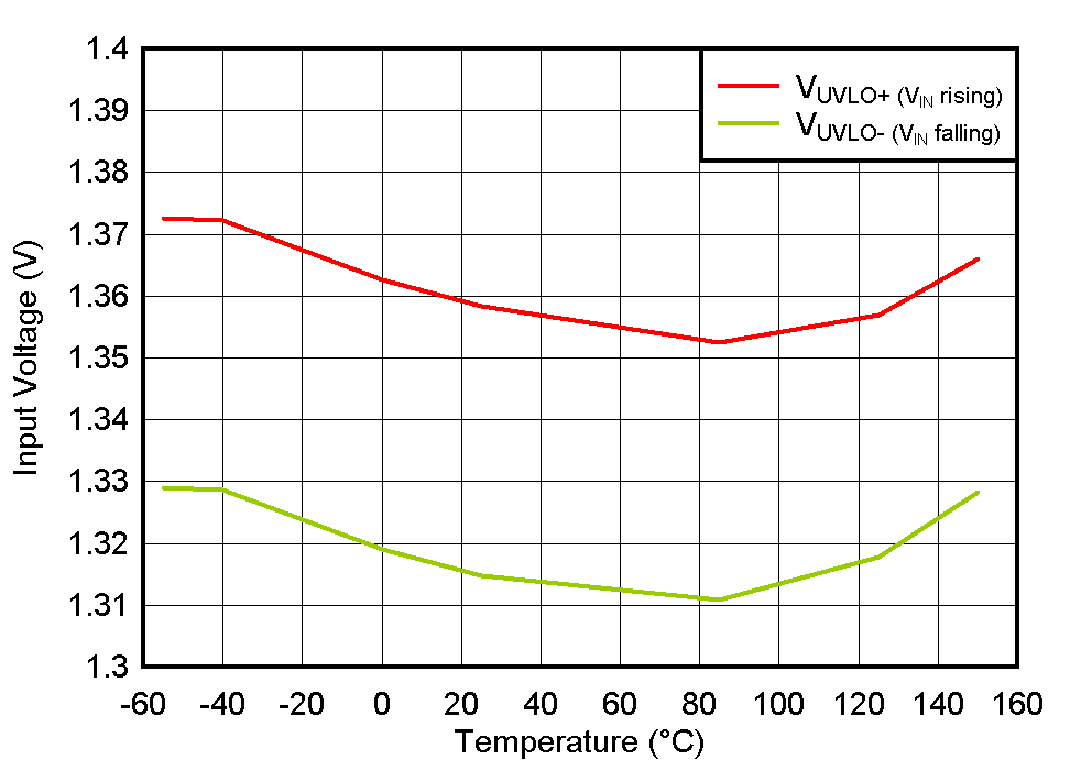
TPS7A20C UVLO Threshold vs Temperature
VEN = 1V
Figure 5-10 UVLO Threshold vs Temperature
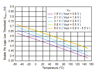
TPS7A20C Enable Logic Low Threshold Low vs Temperature
 
Figure 5-12 Enable Logic Low Threshold Low vs Temperature
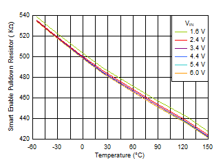
TPS7A20C Smart Enable Pulldown Resistor vs Temperature and VIN
VEN = 0.25V
Figure 5-14 Smart Enable Pulldown Resistor vs Temperature and VIN
TPS7A20C Load Transient
IOUT = 200mA to 50mA, tFALLING = 1µs
Figure 5-16 Load Transient
TPS7A20C Load Transient
IOUT = 200mA to 50mA, tFALLING = 150ns
Figure 5-18 Load Transient
TPS7A20C Load Transient
IOUT = 300mA to 1mA, tFALLING = 1µs
Figure 5-20 Load Transient
TPS7A20C Load Transient
IOUT = 300mA to 1mA, tFALLING = 200ns
Figure 5-22 Load Transient
TPS7A20C Load Transient
IOUT = 300mA to 0mA, tFALLING = 1µs
Figure 5-24 Load Transient
TPS7A20C Load Transient
IOUT = 300mA to 0mA, tFALLING = 200ns
Figure 5-26 Load Transient
TPS7A20C Line Transient
VIN = 3.1V → 4.1V → 3.1V, VIN tRISING = 5µs, IOUT = 300mA
Figure 5-28 Line Transient
TPS7A20C PSRR vs Frequency and VIN
VEN = 1V, IOUT = 20mA, CIN = 0.47µF
Figure 5-30 PSRR vs Frequency and VIN
TPS7A20C Noise vs Frequency and VIN
IOUT = 20mA, VRMS BW = 10Hz to 100kHz
Figure 5-32 Noise vs Frequency and VIN
TPS7A20C Noise vs Frequency and COUT
VIN = 3.85V, IOUT = 20mA, VRMS BW = 10Hz to 100kHz
Figure 5-34 Noise vs Frequency and COUT
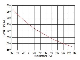
TPS7A20C Start-Up Turn-On Time
VEN = VEN(HI) to VOUT = 95% of VOUT(NOM), IOUT = 0mA
Figure 5-36 Start-Up Turn-On Time
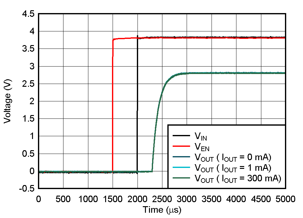
TPS7A20C Start-Up
VIN = 0V to 3.85V, VEN = 0V to 3.85V, VEN rises 500µs ahead of VIN, VIN and VEN slew rate = 1V/µs
Figure 5-38 Start-Up
TPS7A20C Inrush Current
VIN = 3.85V, VEN = 0V to 3.85V, VEN slew rate = 1V/µs, COUT = 10µF
Figure 5-40 Inrush Current