SBVS290B December   2018  – October 2019 TPS7A26

PRODUCTION DATA.  

  1. Features
  2. Applications
  3. Description
    1.     Device Images
      1.      Typical Application Circuit
  4. Revision History
  5. Pin Configuration and Functions
    1.     Pin Functions
  6. Specifications
    1. 6.1 Absolute Maximum Ratings
    2. 6.2 ESD Ratings
    3. 6.3 Recommended Operating Conditions
    4. 6.4 Thermal Information
    5. 6.5 Electrical Characteristics
    6. 6.6 Typical Characteristics
  7. Detailed Description
    1. 7.1 Overview
    2. 7.2 Functional Block Diagram
    3. 7.3 Feature Description
      1. 7.3.1 Output Enable
      2. 7.3.2 Dropout Voltage
      3. 7.3.3 Current Limit
      4. 7.3.4 Undervoltage Lockout (UVLO)
      5. 7.3.5 Thermal Shutdown
      6. 7.3.6 Power Good
      7. 7.3.7 Active Overshoot Pulldown Circuitry
    4. 7.4 Device Functional Modes
      1. 7.4.1 Device Functional Mode Comparison
      2. 7.4.2 Normal Operation
      3. 7.4.3 Dropout Operation
      4. 7.4.4 Disabled
  8. Application and Implementation
    1. 8.1 Application Information
      1. 8.1.1 Adjustable Device Feedback Resistors
      2. 8.1.2 Recommended Capacitor Types
      3. 8.1.3 Input and Output Capacitor Requirements
      4. 8.1.4 Reverse Current
      5. 8.1.5 Feed-Forward Capacitor (CFF)
      6. 8.1.6 Power Dissipation (PD)
      7. 8.1.7 Estimating Junction Temperature
      8. 8.1.8 Special Consideration for Line Transient
    2. 8.2 Typical Application
      1. 8.2.1 Design Requirements
      2. 8.2.2 Detailed Design Procedure
        1. 8.2.2.1 Transient Response
        2. 8.2.2.2 Selecting Feedback Divider Resistors
        3. 8.2.2.3 Thermal Dissipation
      3. 8.2.3 Application Curve
  9. Power Supply Recommendations
  10. 10Layout
    1. 10.1 Layout Guidelines
    2. 10.2 Layout Examples
  11. 11Device and Documentation Support
    1. 11.1 Device Support
      1. 11.1.1 Device Nomenclature
    2. 11.2 Documentation Support
      1. 11.2.1 Related Documentation
    3. 11.3 Receiving Notification of Documentation Updates
    4. 11.4 Community Resources
    5. 11.5 Trademarks
    6. 11.6 Electrostatic Discharge Caution
    7. 11.7 Glossary
  12. 12Mechanical, Packaging, and Orderable Information

Package Options

Refer to the PDF data sheet for device specific package drawings

Mechanical Data (Package|Pins)
  • DRV|6
Thermal pad, mechanical data (Package|Pins)
Orderable Information

Special Consideration for Line Transient

During a line transient, the response of this LDO to a very large or fast input voltage change can cause a brief shutdown lasting up to a few hundred microseconds from the voltage transition. This shutdown can be avoided by reducing the voltage step size, increasing the transition time, or a combination of both. Figure 39 provides a boundary to follow to avoid this behavior. If necessary, reduce slew rate and the voltage step size to stay below the curve.
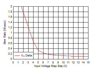
TPS7A26 D043_SBVS290.gifFigure 39. Recommended Input Voltage Step and Slew Rate in a Line transient