SBVS163A June 2011 – May 2015 TPS7A3401
PRODUCTION DATA.
- 1 Features
- 2 Applications
- 3 Description
- 4 Revision History
- 5 Pin Configuration and Functions
- 6 Specifications
- 7 Detailed Description
- 8 Application and Implementation
- 9 Power Supply Recommendations
- 10Layout
- 11Device and Documentation Support
- 12Mechanical, Packaging, and Orderable Information
Package Options
Mechanical Data (Package|Pins)
- DGN|8
Thermal pad, mechanical data (Package|Pins)
- DGN|8
Orderable Information
7 Detailed Description
7.1 Overview
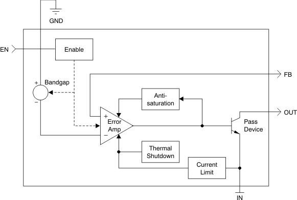
The TPS7A3401 device is a wide VIN, low-noise, 150-mA linear regulator (LDO). This device features an enable pin, programmable soft-start, current limiting, and thermal protection circuitry that allow the device to be used in a wide variety of applications. As a bipolar-based device, the TPS7A3401 device is ideal for high-accuracy, high-precision applications at higher voltages.
7.2 Functional Block Diagram

7.3 Feature Description
7.3.1 Internal Current Limit
The fixed internal current limit of the TPS7A3401 device helps protect the regulator during fault conditions. The maximum amount of current the device can source is the current limit (330 mA, typical), and it is largely independent of output voltage. For reliable operation, do not operate the device in current limit for extended periods of time.
7.3.2 Enable Pin Operation
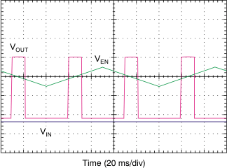
The TPS7A3401 device provides a dual polarity enable pin (EN) that turns on the regulator when |VEN| > 2 V, whether the voltage is positive or negative, as shown in Figure 18.
This functionality allows for different system power management topologies:
- Connecting the EN pin directly to a negative voltage, such as VIN, or
- Connecting the EN pin directly to a positive voltage, such as the output of digital logic circuitry.
 Figure 18. Enable Pin Positive and Negative Threshold
7.4 Device Functional Modes
7.4.1 Normal Operation
The device regulates to the nominal output voltage under the following conditions:
- The input voltage is at least as high as the |VIN(min)|.
- The input voltage magnitude is greater than the nominal output voltage magnitude added to the dropout voltage.
- |VEN| > |VEN(HI)|
- The output current is less than the current limit.
- The device junction temperature is less than the maximum specified junction temperature.
7.4.2 Dropout Operation
If the input voltage magnitude is lower than the nominal output voltage magnitude plus the specified dropout voltage magnitude, but all other conditions are met for normal operation, the device operates in dropout mode. In this mode of operation, the output voltage magnitude is the same as the input voltage magnitude minus the dropout voltage magnitude. The transient performance of the device is significantly degraded because the pass device (as a bipolar junction transistor, or BJT) is in saturation and no longer controls the current through the LDO. Line or load transients in dropout can result in large output voltage deviations.
7.4.3 Disabled
The device is disabled under the following conditions:
- |VEN| < |VEN(HI)|
- The device junction temperature is greater than the thermal shutdown temperature.
Table 1 shows the conditions that lead to the different modes of operation.
Table 1. Device Functional Mode Comparison
| OPERATING MODE | PARAMETER | |||
|---|---|---|---|---|
| VIN | VEN | IOUT | TJ | |
| Normal mode | |VIN| > { |VOUT(nom)| + |VDO|, |VIN(min)| } | |VEN| > |V(HI)| | I OUT < ICL | T J < 125°C |
| Dropout mode | |VIN(min)| < |VIN| < |VOUT(nom)| + |VDO| | |VEN| > |V(HI)| | — | TJ < 125°C |
| Disabled mode (any true condition disables the device) |
— | |VEN| < |V(HI)| | — | TJ > 170°C |