SBVS393B
December 2020 – November 2022
TPS7A43
PRODUCTION DATA
1
Features
2
Applications
3
Description
4
Revision History
5
Pin Configuration and Functions
6
Specifications
6.1
Absolute Maximum Ratings
6.2
ESD Ratings
6.3
Recommended Operating Conditions
6.4
Thermal Information
6.5
Electrical Characteristics
6.6
Typical Characteristics
7
Detailed Description
7.1
Overview
7.2
Functional Block Diagrams
7.3
Feature Description
7.3.1
MID_OUT Voltage Selection
7.3.2
Precision Enable
7.3.3
Dropout Voltage
7.3.4
Current Limit
7.3.5
Thermal Shutdown
7.3.6
Power Good
7.4
Device Functional Modes
7.4.1
Device Functional Mode Comparison
7.4.2
Normal Operation
7.4.3
Dropout Operation
7.4.4
Disabled
8
Application and Implementation
8.1
Application Information
8.1.1
MID_OUT Voltage Setting
8.1.2
Adjustable Device Feedback Resistors
8.1.3
Recommended Capacitor Types
8.1.4
Input and Output Capacitor Requirements
8.1.5
Power Dissipation (PD)
8.1.6
Estimating Junction Temperature
8.2
Typical Application
8.2.1
Design Requirements
8.2.2
Detailed Design Procedure
8.2.3
Application Curves
8.3
Power Supply Recommendations
8.4
Layout
8.4.1
Layout Guidelines
8.4.2
Layout Examples
9
Device and Documentation Support
9.1
Device Support
9.1.1
Development Support
9.1.1.1
Evaluation Modules
9.1.1.2
Spice Models
9.1.2
Device Nomenclature
9.2
Documentation Support
9.2.1
Related Documentation
9.3
Receiving Notification of Documentation Updates
9.4
Support Resources
9.5
Trademarks
9.6
Electrostatic Discharge Caution
9.7
Glossary
10
Mechanical, Packaging, and Orderable Information
Package Options
Mechanical Data (Package|Pins)
DGQ|10
MPDS043F
Thermal pad, mechanical data (Package|Pins)
DGQ|10
PPTD325B
Orderable Information
sbvs393b_oa
sbvs393b_pm
8.4.2
Layout Examples
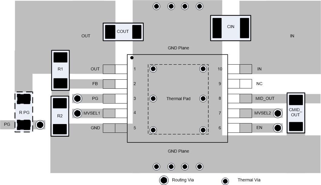
Figure 8-4
Adjustable Version Layout Example
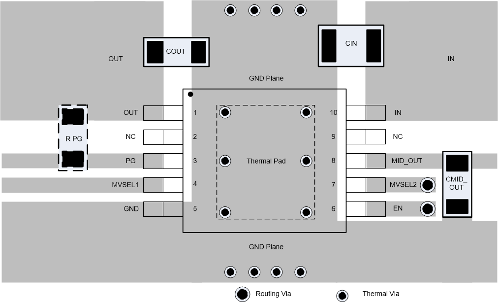
Figure 8-5
Fixed Version Layout Example