SBVS421 November   2021 TPS7A44

PRODUCTION DATA  

  1. Features
  2. Applications
  3. Description
  4. Revision History
  5. Pin Configuration and Functions
  6. Specifications
    1. 6.1 Absolute Maximum Ratings
    2. 6.2 ESD Ratings
    3. 6.3 Recommended Operating Conditions
    4. 6.4 Thermal Information
    5. 6.5 Electrical Characteristics
    6. 6.6 Typical Characteristics
  7. Detailed Description
    1. 7.1 Overview
    2. 7.2 Functional Block Diagrams
    3. 7.3 Feature Description
      1. 7.3.1 MID_OUT Voltage Selection
      2. 7.3.2 Precision Enable
      3. 7.3.3 Dropout Voltage
      4. 7.3.4 Current Limit
      5. 7.3.5 Thermal Shutdown
      6. 7.3.6 Power Good
    4. 7.4 Device Functional Modes
      1. 7.4.1 Device Functional Mode Comparison
      2. 7.4.2 Normal Operation
      3. 7.4.3 Dropout Operation
      4. 7.4.4 Disabled
  8. Application and Implementation
    1. 8.1 Application Information
      1. 8.1.1 MID_OUT Voltage Setting
      2. 8.1.2 Adjustable Device Feedback Resistors
      3. 8.1.3 Recommended Capacitor Types
      4. 8.1.4 Input and Output Capacitor Requirements
      5. 8.1.5 Power Dissipation (PD)
      6. 8.1.6 Estimating Junction Temperature
    2. 8.2 Typical Application
      1. 8.2.1 Design Requirements
      2. 8.2.2 Detailed Design Procedure
      3. 8.2.3 Application Curves
  9. Power Supply Recommendations
  10. 10Layout
    1. 10.1 Layout Guidelines
    2. 10.2 Layout Examples
  11. 11Device and Documentation Support
    1. 11.1 Device Support
      1. 11.1.1 Development Support
        1. 11.1.1.1 Evaluation Modules
        2. 11.1.1.2 Spice Models
      2. 11.1.2 Device Nomenclature
    2. 11.2 Documentation Support
      1. 11.2.1 Related Documentation
    3. 11.3 Receiving Notification of Documentation Updates
    4. 11.4 Support Resources
    5. 11.5 Trademarks
    6. 11.6 Electrostatic Discharge Caution
    7. 11.7 Glossary
  12. 12Mechanical, Packaging, and Orderable Information

Package Options

Mechanical Data (Package|Pins)
Thermal pad, mechanical data (Package|Pins)
Orderable Information

Application Curves

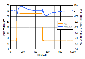
GUID-20210907-SS0I-DHFV-LTTQ-8H8DHPCF4MRR-low.gif
VIN = 15 V to 65 V, VIN ramp rate = 10 V/μs, VMVSEL1 = 0 V, VMVSEL2 = 0.9 V, IOUT = 50 mA, IMID_OUT = open
Figure 8-2 TPS7A43 Line Transient: 15 V to 65 V
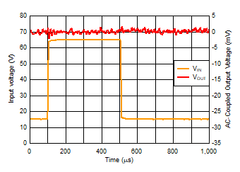
GUID-20210907-SS0I-HXJT-14P3-DPDLSF5FHQPQ-low.gif
VIN = 15 V to 65 V, VIN ramp rate = 10 V/μs, VMVSEL1 = 0 V, VMVSEL2 = 0.9 V, IOUT = 50 mA, IMID_OUT = open
Figure 8-3 TPS7A43 Line Transient: 15 V to 65 V (Zoom on VOUT)