SBVS295A November 2019 – March 2020 TPS7A52
PRODUCTION DATA.
- 1 Features
- 2 Applications
- 3 Description
- 4 Revision History
- 5 Pin Configuration and Functions
- 6 Specifications
- 7 Detailed Description
-
8 Application and Implementation
- 8.1
Application Information
- 8.1.1 Recommended Capacitor Types
- 8.1.2 Soft Start and Inrush Current
- 8.1.3 Optimizing Noise and PSRR
- 8.1.4 Charge Pump Noise
- 8.1.5 Current Sharing
- 8.1.6 Adjustable Operation
- 8.1.7 Power-Good Operation
- 8.1.8 Undervoltage Lockout (UVLO) Operation
- 8.1.9 Dropout Voltage (VDO)
- 8.1.10 Device Behavior During Transition From Dropout Into Regulation
- 8.1.11 Load Transient Response
- 8.1.12 Reverse Current Protection Considerations
- 8.1.13 Power Dissipation (PD)
- 8.1.14 Estimating Junction Temperature
- 8.1.15 TPS7A52EVM Thermal Analysis
- 8.2 Typical Application
- 8.1
Application Information
- 9 Power Supply Recommendations
- 10Layout
- 11Device and Documentation Support
- 12Mechanical, Packaging, and Orderable Information
Package Options
Mechanical Data (Package|Pins)
- RPS|12
Thermal pad, mechanical data (Package|Pins)
Orderable Information
8.1.11 Load Transient Response
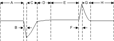
The load-step transient response is the output voltage response by the LDO to a step in load current, whereby output voltage regulation is maintained. There are two key transitions during a load transient response: the transition from a light to a heavy load, and the transition from a heavy to a light load. The regions shown in Figure 32 are broken down in this section. Regions A, E, and H are where the output voltage is in steady-state regulation.
 Figure 32. Load Transient Waveform
 During transitions from a light load to a heavy load:
- Initial voltage dip is a result of the depletion of the output capacitor charge and parasitic impedance to the output capacitor (region B).
- Recovery from the dip results from the LDO increasing its sourcing current, and leads to output voltage regulation (region C).
During transitions from a heavy load to a light load:
- Initial voltage rise results from the LDO sourcing a large current, and leads to the output capacitor charge to increase (region F).
- Recovery from the rise results from the LDO decreasing its sourcing current in combination with the load discharging the output capacitor (region G).
Transitions between current levels changes the internal power dissipation because the TPS7A52 is a high-current device (region D). The change in power dissipation changes the die temperature during these transitions, and leads to a slightly different voltage level. This different output voltage level shows up in the various load transient responses.
A larger output capacitance reduces the peaks during a load transient but slows down the response time of the device. A larger dc load also reduces the peaks because the amplitude of the transition is lowered and a higher current discharge path is provided for the output capacitor.