SBVS412A November   2022  – December 2022 TPS7A53A-Q1

PRODUCTION DATA  

  1. Features
  2. Applications
  3. Description
  4. Revision History
  5. Pin Configuration and Functions
  6. Specifications
    1. 6.1 Absolute Maximum Ratings
    2. 6.2 ESD Ratings
    3. 6.3 Recommended Operating Conditions
    4. 6.4 Thermal Information
    5. 6.5 Electrical Characteristics
    6. 6.6 Typical Characteristics
  7. Detailed Description
    1. 7.1 Overview
    2. 7.2 Functional Block Diagram
    3. 7.3 Feature Description
      1. 7.3.1 Enable and Shutdown
      2. 7.3.2 Active Discharge
      3. 7.3.3 Power-Good Output (PG)
      4. 7.3.4 Internal Current Limit
      5. 7.3.5 Thermal Shutdown Protection (TSD)
    4. 7.4 Device Functional Modes
      1. 7.4.1 Normal Operation
      2. 7.4.2 Dropout Operation
      3. 7.4.3 Disabled
  8. Application and Implementation
    1. 8.1 Application Information
      1. 8.1.1 Input, Output, and Bias Capacitor Requirements
      2. 8.1.2 Dropout Voltage
      3. 8.1.3 Output Noise
      4. 8.1.4 Estimating Junction Temperature
      5. 8.1.5 Soft Start, Sequencing, and Inrush Current
      6. 8.1.6 Power-Good Operation
    2. 8.2 Typical Application
      1. 8.2.1 Design Requirements
      2. 8.2.2 Detailed Design Procedure
      3. 8.2.3 Application Curve
    3. 8.3 Power Supply Recommendations
    4. 8.4 Layout
      1. 8.4.1 Layout Guidelines
        1. 8.4.1.1 Board Layout
        2. 8.4.1.2 RTJ Package — High CTE Mold Compound
      2. 8.4.2 Layout Example
  9. Device and Documentation Support
    1. 9.1 Documentation Support
      1. 9.1.1 Related Documentation
    2. 9.2 Receiving Notification of Documentation Updates
    3. 9.3 Support Resources
    4. 9.4 Trademarks
    5. 9.5 Electrostatic Discharge Caution
    6. 9.6 Glossary
  10. 10Mechanical, Packaging, and Orderable Information
    1. 10.1 Mechanical Data

Package Options

Refer to the PDF data sheet for device specific package drawings

Mechanical Data (Package|Pins)
  • RTJ|20
Thermal pad, mechanical data (Package|Pins)
Orderable Information

Typical Application

This section discusses the implementation of the fixed 1.0-V TPS7A53A-Q1 to regulate a 3-A load requiring good PSRR at high frequency with low noise. Figure 8-3 provides a schematic for this typical application circuit.
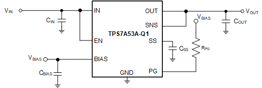
GUID-20221108-SS0I-3F9S-1GLF-H7NNNCJRTPW3-low.gif Figure 8-3 Typical Fixed Voltage Application