SBVS412A November 2022 – December 2022 TPS7A53A-Q1
PRODUCTION DATA
- 1 Features
- 2 Applications
- 3 Description
- 4 Revision History
- 5 Pin Configuration and Functions
- 6 Specifications
- 7 Detailed Description
- 8 Application and Implementation
- 9 Device and Documentation Support
- 10Mechanical, Packaging, and Orderable Information
Package Options
Refer to the PDF data sheet for device specific package drawings
Mechanical Data (Package|Pins)
- RTJ|20
Thermal pad, mechanical data (Package|Pins)
Orderable Information
3 Description
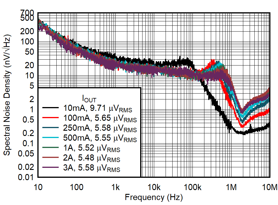
The TPS7A53A-Q1 is a low-noise (5.6 µVRMS), low-dropout linear regulator (LDO) capable of sourcing 3 A with only 130 mV of dropout.
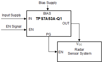
The combination of low noise (5.6 µVRMS), high PSRR, and high output current capability makes the TPS7A53A-Q1 designed for powering noise-sensitive components, such as those found in radar power and infotainment applications. The high performance of this device limits power-supply-generated phase noise and clock jitter, making this device useful for powering RF amplifiers, radar sensors, and chipsets. Specifically, signal chain components benefit from the high-performance of the device. The TPS7A53A-Q1 is available with a wettable flanks option to facilitate optical inspection.
For digital loads [such as application-specific integrated circuits (ASICs), field-programmable gate arrays (FPGAs), and digital signal processors (DSPs)] that require low-input, low-output (LILO) voltage operation, the exceptional accuracy (1.3% over load and temperature), remote sensing, excellent transient performance, and soft-start capabilities of the TPS7A53A-Q1 provide optimal system performance.
The versatility of the TPS7A53A-Q1 makes the device a component of choice for many demanding applications.
| PART NUMBER | PACKAGE | BODY SIZE (NOM) |
|---|---|---|
| TPS7A53A-Q1 | RTJ (WQFN, 20) with wettable flank |
4.00 mm × 4.00 mm |
 Powering RF
Components
 Spectral Noise Density vs
Frequency and Output Current