SBVS395 July 2022 TPS7A57
PRODUCTION DATA
- 1 Features
- 2 Applications
- 3 Description
- 4 Revision History
- 5 Pin Configuration and Functions
- 6 Specifications
-
7 Detailed Description
- 7.1 Overview
- 7.2 Functional Block Diagram
- 7.3
Feature Description
- 7.3.1 Output Voltage Setting and Regulation
- 7.3.2 Low-Noise, Ultra-High Power-Supply Rejection Ratio (PSRR)
- 7.3.3 Programmable Soft-Start (NR/SS Pin)
- 7.3.4 Precision Enable and UVLO
- 7.3.5 Charge Pump Enable and BIAS Rail
- 7.3.6 Power-Good Pin (PG Pin)
- 7.3.7 Active Discharge
- 7.3.8 Thermal Shutdown Protection (TSD)
- 7.4 Device Functional Modes
-
8 Application and Implementation
- 8.1
Application Information
- 8.1.1 Precision Enable (External UVLO)
- 8.1.2 Undervoltage Lockout (UVLO) Operation
- 8.1.3 Dropout Voltage (VDO)
- 8.1.4 Input and Output Capacitor Requirements (CIN and COUT)
- 8.1.5 Recommended Capacitor Types
- 8.1.6 Soft-Start, Noise Reduction (NR/SS Pin), and Power-Good (PG Pin)
- 8.1.7 Optimizing Noise and PSRR
- 8.1.8 Adjustable Operation
- 8.1.9 Load Transient Response
- 8.1.10 Current Limit and Foldback Behavior
- 8.1.11 Charge Pump Operation
- 8.1.12 Sequencing
- 8.1.13 Power-Good Functionality
- 8.1.14 Output Impedance
- 8.1.15 Paralleling for Higher Output Current and Lower Noise
- 8.1.16 Current Mode Margining
- 8.1.17 Voltage Mode Margining
- 8.1.18 Power Dissipation (PD)
- 8.1.19 Estimating Junction Temperature
- 8.1.20 TPS7A57EVM-081 Thermal Analysis
- 8.2 Typical Application
- 8.3 Power Supply Recommendations
- 8.4 Layout
- 8.1
Application Information
- 9 Device and Documentation Support
- 10Mechanical, Packaging, and Orderable Information
Package Options
Mechanical Data (Package|Pins)
- RTE|16
Thermal pad, mechanical data (Package|Pins)
- RTE|16
Orderable Information
8.1.14 Output Impedance
Output impedance can be modeled, as shown in Figure 8-13, as an ideal voltage source followed by a series R (ROUT) and series L (LOUT) output.
 Figure 8-13 Output Impedance Model
Output impedance curves were measured using the EVM and are provided for the following conditions:
- Figure 8-14, Figure 8-15, and Figure 8-16 are provided for the 5.5-VIN, 5-VOUT, and IOUT = 200-mA, 500-mA, and 5-A conditions
- Figure 8-17 is provided for the 0.9-VIN, 0.5-VOUT, and IOUT = 4.6-A conditions
- Figure 8-18 to Figure 8-21 are provided for the 0.75 -VIN, 0.5-VOUT, 3-VBIAS, and IOUT = 20-mA, 200-mA, 500-mA, and 1-A conditions.
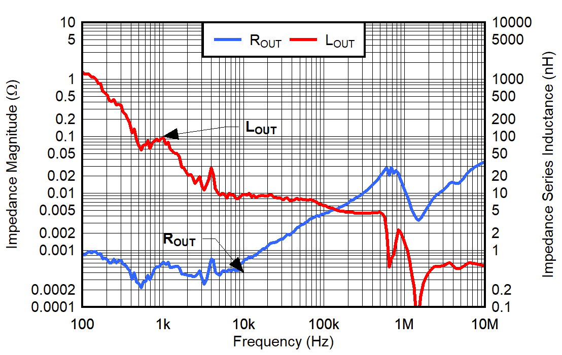 Figure 8-14 VIN = 5.5 V,
VOUT = 5 V, VBIAS = 8 V, CP_EN = 0,
IOUT = 200 mA
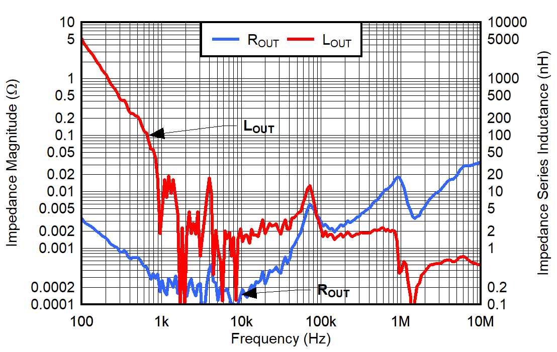 Figure 8-16 VIN = 5.5 V,
VOUT = 5 V, VBIAS = 8 V, CP_EN = 0,
IOUT = 5 A
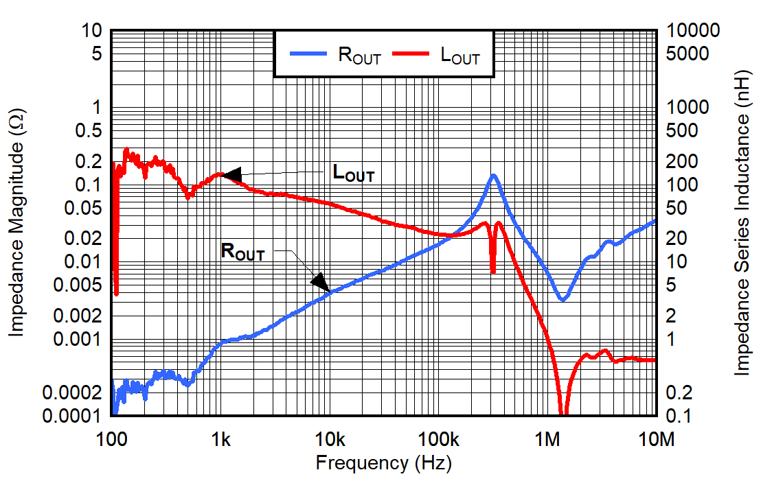 Figure 8-18 VIN = 0.75 V,
VBIAS = 3 V, VOUT = 0.5 V , CP_EN = 0,
IOUT = 20 mA
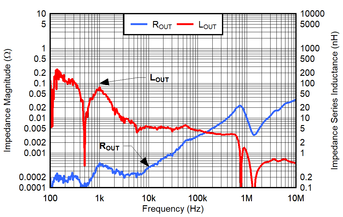 Figure 8-20 VIN = 0.75 V,
VBIAS = 3 V, VOUT = 0.5 V, CP_EN = 0,
IOUT = 500 mA
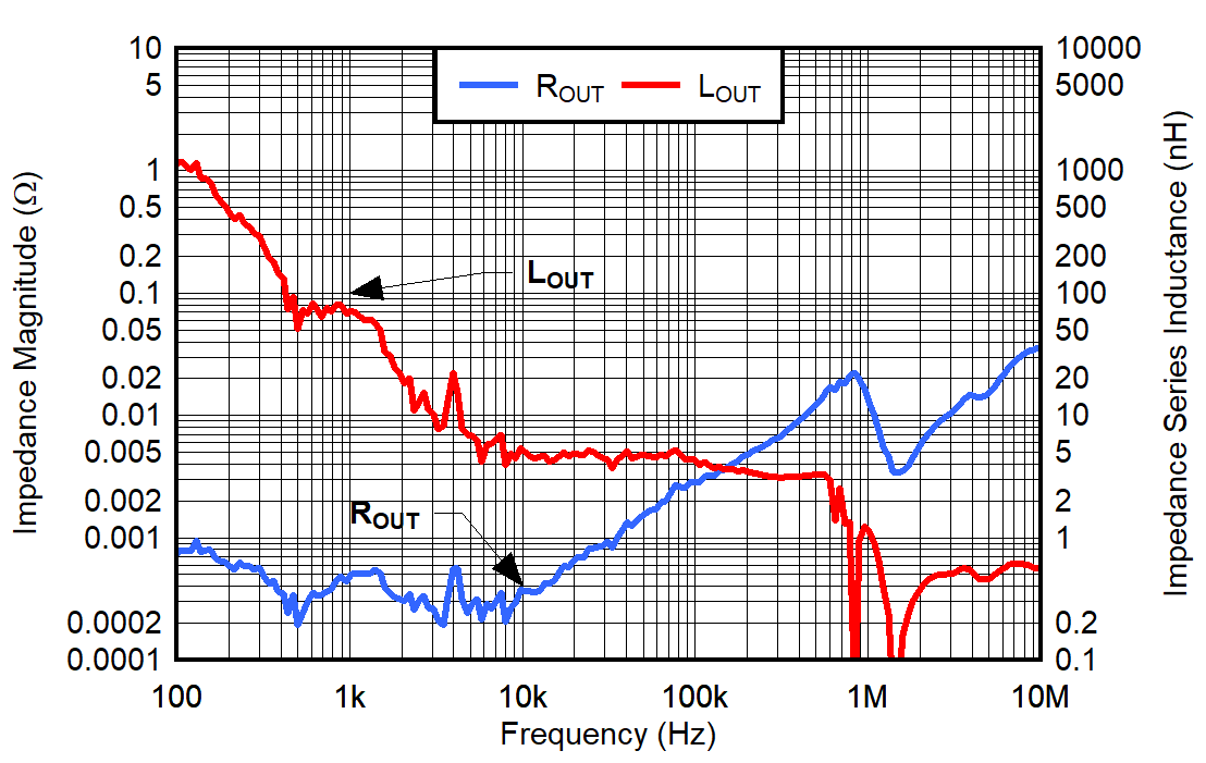 Figure 8-15 VIN = 5.5 V,
VOUT = 5 V, VBIAS = 8 V, CP_EN = 0,
IOUT = 500 mA
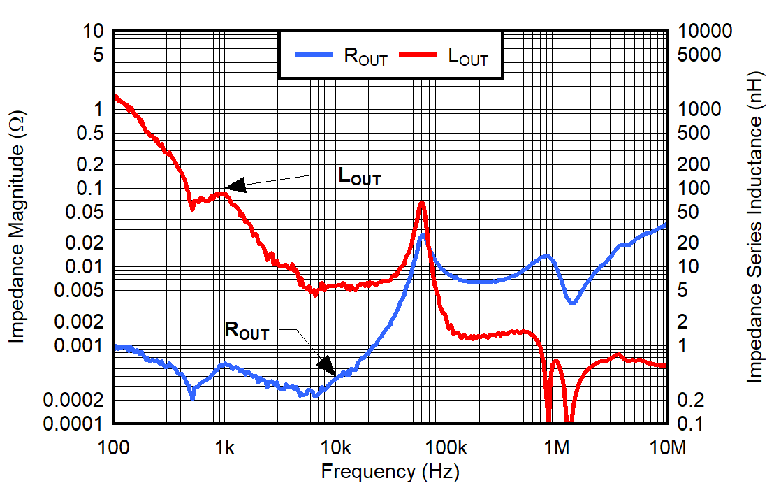 Figure 8-17 VIN = 0.9 V,
VBIAS = 3 V, VOUT = 0.5 V , CP_EN = 0,
IOUT = 4.6 A
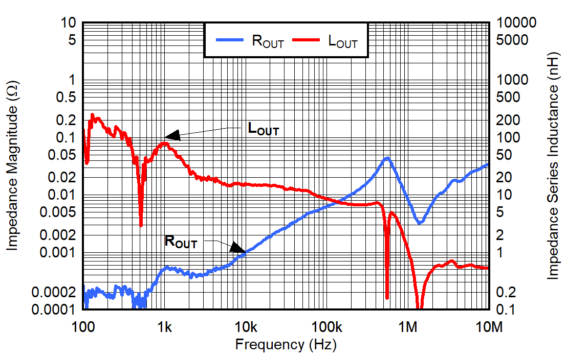 Figure 8-19 VIN = 0.75 V,
VBIAS = 3 V, VOUT = 0.5 V, CP_EN = 0,
IOUT = 100 mA
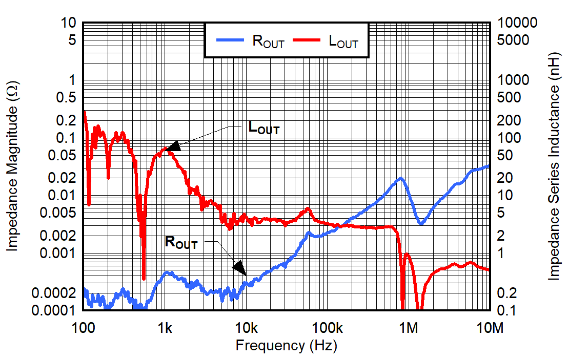 Figure 8-21 VIN = 0.75 V,
VBIAS = 3 V, VOUT = 0.5 V, CP_EN = 0,
IOUT = 1 A
Figure 8-21 VIN = 0.75 V,
VBIAS = 3 V, VOUT = 0.5 V, CP_EN = 0,
IOUT = 1 ATable 8-6 provides a summary of the tested conditions described in this section.
Table 8-6 Model for Tested Conditions
Summary
| VIN | VOUT | VBIAS | IOUT | CP_EN | ROUT | LOUT |
|---|---|---|---|---|---|---|
| 0.75 V | 0.5 V | 3 V | 20 mA | Off | 200 μΩ | 0.5 nH |
| 0.75 V | 0.5 V | 3 V | 200 mA | Off | 200 μΩ | 0.5 nH |
| 0.75 V | 0.5 V | 3 V | 500 mA | Off | 200 μΩ | 0.5 nH |
| 0.75 V | 0.5 V | 3 V | 1 A | Off | 200 μΩ | 0.5 nH |
| 0.9 V | 0.5 V | 3 V | 4.6 A | Off | 200 μΩ | 0.5 nH |
| 5.5 V | 5 V | 8 V | 200 mA | Off | 400 μΩ | 0.5 nH |
| 5.5 V | 5 V | 8 V | 500 mA | Off | 300 μΩ | 0.5 nH |
| 5.5 V | 5 V | 8 V | 5 A | Off | 200 μΩ | 0.5 nH |