SLVSAA0E November 2010 – March 2020 TPS7A6201-Q1
PRODUCTION DATA.
- 1 Features
- 2 Applications
- 3 Description
- 4 Revision History
- 5 Pin Configuration and Functions
- 6 Specifications
- 7 Detailed Description
- 8 Application and Implementation
- 9 Power Supply Recommendations
- 10Layout
- 11Device and Documentation Support
- 12Mechanical, Packaging, and Orderable Information
Package Options
Refer to the PDF data sheet for device specific package drawings
Mechanical Data (Package|Pins)
- KTT|5
Thermal pad, mechanical data (Package|Pins)
- KTT|5
Orderable Information
6.6 Typical Characteristics
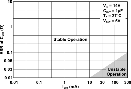 Figure 1. ESR vs Load Current
 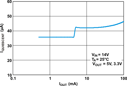 Figure 3. Quiescent Current vs Load Current
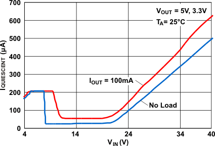
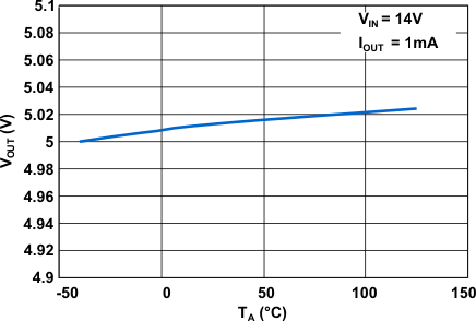 Figure 7. Output Voltage vs Ambient Air Temperature
(VOUT Programmed to 5 V)
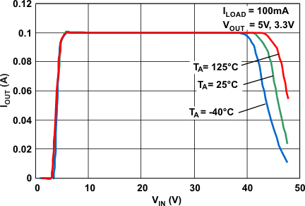 Figure 9. Output Current vs Input Voltage
 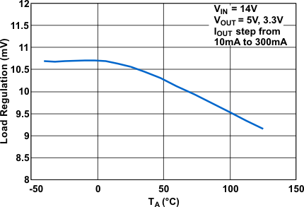 Figure 11. Load Regulation vs Ambient Air Temperature
 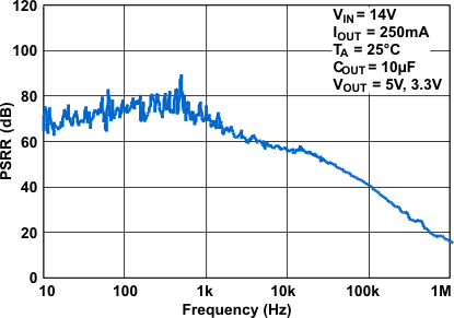 Figure 13. PSRR at Heavy Load Current
 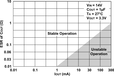 Figure 2. ESR vs Load Current
 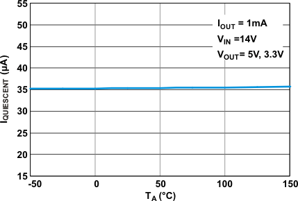 Figure 4. Quiescent Current vs Ambient Air Temperature
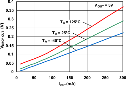
| Dropout voltage is measured when the output voltage drops by 100 mV from the regulated output voltage level. (For example, if output voltage is programmed to be 5 V, the dropout voltage is measured when the output voltage drops down to 4.9 V from 5 V.) |
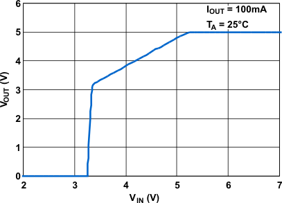 Figure 8. Output Voltage vs Input Voltage
(VOUT Programmed to 5 V)
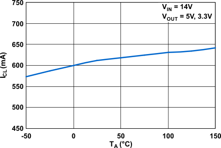 Figure 10. Output Current Limit vs
Ambient Air Temperature
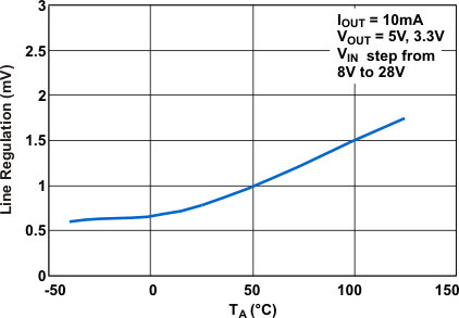 Figure 12. Line Regulation vs Ambient Air Temperature
 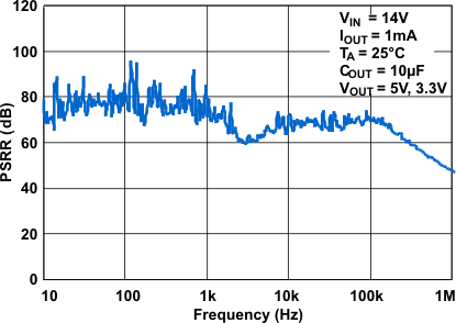 Figure 14. PSRR at Light Load Current