SLVSAB1G June   2011  – March 2020 TPS7A63-Q1 , TPS7A6401-Q1

PRODUCTION DATA.  

  1. Features
  2. Applications
  3. Description
    1.     Device Images
      1.      Fixed Output Voltage Option
      2.      Adjustable Output Voltage Option
  4. Revision History
  5. Pin Configuration and Functions
    1.     Pin Functions
  6. Specifications
    1. 6.1 Absolute Maximum Ratings
    2. 6.2 ESD Ratings
    3. 6.3 Recommended Operating Conditions
    4. 6.4 Thermal Information
    5. 6.5 Electrical Characteristics
    6. 6.6 Typical Characteristics
  7. Detailed Description
    1. 7.1 Overview
    2. 7.2 Functional Block Diagrams
    3. 7.3 Feature Description
      1. 7.3.1  Power Up, Reset Delay, and Reset Output
      2. 7.3.2  Adjustable Output Voltage
      3. 7.3.3  Chip Enable
      4. 7.3.4  Charge Pump Operation
      5. 7.3.5  Low-Power Mode
      6. 7.3.6  Undervoltage Shutdown
      7. 7.3.7  Low-Voltage Tracking
      8. 7.3.8  Integrated Fault Protection
      9. 7.3.9  Thermal Shutdown
      10. 7.3.10 Integrated Window Watchdog
        1. 7.3.10.1 Programmable-Window Watchdog
        2. 7.3.10.2 Watchdog Enable
        3. 7.3.10.3 Watchdog Service Signal
        4. 7.3.10.4 Watchdog Fault Outputs
        5. 7.3.10.5 Watchdog Initialization
        6. 7.3.10.6 Watchdog Operation
        7. 7.3.10.7 Watchdog Fault Conditions
    4. 7.4 Device Functional Modes
      1. 7.4.1 Operation With VIN Lower Than 4 V
      2. 7.4.2 Operation With VIN Larger Than 4 V
  8. Application and Implementation
    1. 8.1 Application Information
      1. 8.1.1 Example
    2. 8.2 Typical Applications
      1. 8.2.1 Typical Application Using the TPS7A6333-Q1 or TPS7A6350-Q1
        1. 8.2.1.1 Design Requirements
        2. 8.2.1.2 Detailed Design Procedure
        3. 8.2.1.3 Application Curves
      2. 8.2.2 Typical Application Using the TPS7A6401-Q1
        1. 8.2.2.1 Design Requirements
        2. 8.2.2.2 Detailed Design Procedure
        3. 8.2.2.3 Application Curves
  9. Power Supply Recommendations
  10. 10Layout
    1. 10.1 Layout Guidelines
      1. 10.1.1 Power Dissipation and Thermal Considerations
        1. 10.1.1.1 Example
    2. 10.2 Layout Example
  11. 11Device and Documentation Support
    1. 11.1 Related Links
    2. 11.2 Receiving Notification of Documentation Updates
    3. 11.3 Community Resources
    4. 11.4 Trademarks
    5. 11.5 Electrostatic Discharge Caution
    6. 11.6 Glossary
  12. 12Mechanical, Packaging, and Orderable Information

Package Options

Mechanical Data (Package|Pins)
Thermal pad, mechanical data (Package|Pins)
Orderable Information

Thermal Shutdown

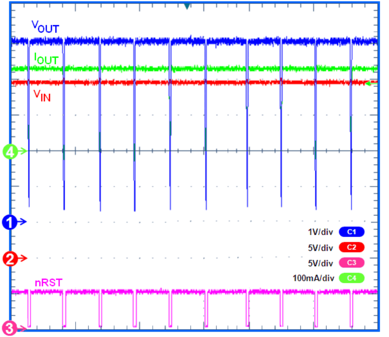
These devices incorporate a thermal shutdown (TSD) circuit as a protection from overheating. For continuous normal operation, the junction temperature should not exceed the TSD trip point. The junction temperature exceeding the TSD trip point causes the output to turn off. When the junction temperature falls below TSD trip point, the output turns on again, as Figure 21 shows.
TPS7A63-Q1 TPS7A6401-Q1 x_tracking_lvsab1.gifFigure 20. Low-Voltage Tracking and Undervoltage Lockout
TPS7A63-Q1 TPS7A6401-Q1 tsd_lvsab1.gif
Figure 21. Thermal Cycling Waveform for TPS7A6350-Q1 (VIN= 24 V, IOUT= 200 mA, VOUT= 5 V)