SLVSAB1G June   2011  – March 2020 TPS7A63-Q1 , TPS7A6401-Q1

PRODUCTION DATA.  

  1. Features
  2. Applications
  3. Description
    1.     Device Images
      1.      Fixed Output Voltage Option
      2.      Adjustable Output Voltage Option
  4. Revision History
  5. Pin Configuration and Functions
    1.     Pin Functions
  6. Specifications
    1. 6.1 Absolute Maximum Ratings
    2. 6.2 ESD Ratings
    3. 6.3 Recommended Operating Conditions
    4. 6.4 Thermal Information
    5. 6.5 Electrical Characteristics
    6. 6.6 Typical Characteristics
  7. Detailed Description
    1. 7.1 Overview
    2. 7.2 Functional Block Diagrams
    3. 7.3 Feature Description
      1. 7.3.1  Power Up, Reset Delay, and Reset Output
      2. 7.3.2  Adjustable Output Voltage
      3. 7.3.3  Chip Enable
      4. 7.3.4  Charge Pump Operation
      5. 7.3.5  Low-Power Mode
      6. 7.3.6  Undervoltage Shutdown
      7. 7.3.7  Low-Voltage Tracking
      8. 7.3.8  Integrated Fault Protection
      9. 7.3.9  Thermal Shutdown
      10. 7.3.10 Integrated Window Watchdog
        1. 7.3.10.1 Programmable-Window Watchdog
        2. 7.3.10.2 Watchdog Enable
        3. 7.3.10.3 Watchdog Service Signal
        4. 7.3.10.4 Watchdog Fault Outputs
        5. 7.3.10.5 Watchdog Initialization
        6. 7.3.10.6 Watchdog Operation
        7. 7.3.10.7 Watchdog Fault Conditions
    4. 7.4 Device Functional Modes
      1. 7.4.1 Operation With VIN Lower Than 4 V
      2. 7.4.2 Operation With VIN Larger Than 4 V
  8. Application and Implementation
    1. 8.1 Application Information
      1. 8.1.1 Example
    2. 8.2 Typical Applications
      1. 8.2.1 Typical Application Using the TPS7A6333-Q1 or TPS7A6350-Q1
        1. 8.2.1.1 Design Requirements
        2. 8.2.1.2 Detailed Design Procedure
        3. 8.2.1.3 Application Curves
      2. 8.2.2 Typical Application Using the TPS7A6401-Q1
        1. 8.2.2.1 Design Requirements
        2. 8.2.2.2 Detailed Design Procedure
        3. 8.2.2.3 Application Curves
  9. Power Supply Recommendations
  10. 10Layout
    1. 10.1 Layout Guidelines
      1. 10.1.1 Power Dissipation and Thermal Considerations
        1. 10.1.1.1 Example
    2. 10.2 Layout Example
  11. 11Device and Documentation Support
    1. 11.1 Related Links
    2. 11.2 Receiving Notification of Documentation Updates
    3. 11.3 Community Resources
    4. 11.4 Trademarks
    5. 11.5 Electrostatic Discharge Caution
    6. 11.6 Glossary
  12. 12Mechanical, Packaging, and Orderable Information

Package Options

Mechanical Data (Package|Pins)
Thermal pad, mechanical data (Package|Pins)
Orderable Information

Typical Characteristics

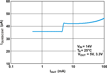
TPS7A63-Q1 TPS7A6401-Q1 g_iq_iout_lvsab1.gif
Figure 1. Quiescent Current vs Load Current
TPS7A63-Q1 TPS7A6401-Q1 g_iq_vin_lvsab1.gif
Figure 3. Quiescent Current vs Input Voltage
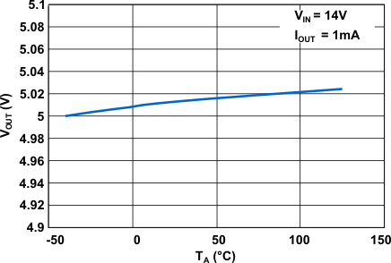
TPS7A63-Q1 TPS7A6401-Q1 g_vout_ta_lvsab1.gif
Figure 5. Output Voltage vs Ambient Air Temperature (VOUT Set To 5 V)
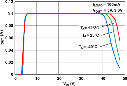
TPS7A63-Q1 TPS7A6401-Q1 g_iout_vin_lvsab1.gif
Figure 7. Output Voltage vs Input Voltage
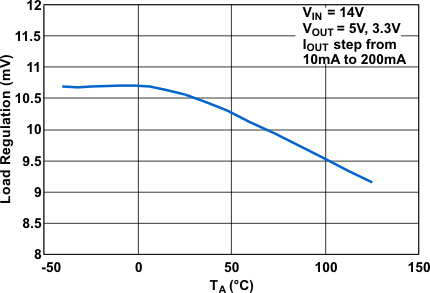
TPS7A63-Q1 TPS7A6401-Q1 g_loadreg_ta_lvsab1.gif
Figure 9. Load Regulation vs Ambient Air Temperature
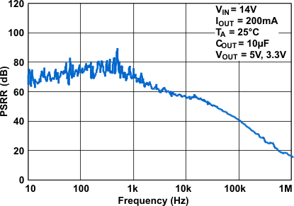
TPS7A63-Q1 TPS7A6401-Q1 g_psrr_heavy_lvsab1.gif
Figure 11. PSRR at Heavy Load Current
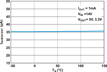
TPS7A63-Q1 TPS7A6401-Q1 g_iq_ta_lvsab1.gif
Figure 2. Quiescent Current vs Ambient Air Temperature
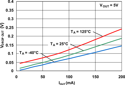
TPS7A63-Q1 TPS7A6401-Q1 g_vdo_iout_lvsab1.gif
Measure dropout voltage when the output voltage drops by 100 mV from the regulated output-voltage level. (For example, for an output voltage programmed to be 5 V, measure the dropout voltage when the output voltage drops down to 4.9 V from 5 V.)
Figure 4. Dropout Voltage vs Load Current
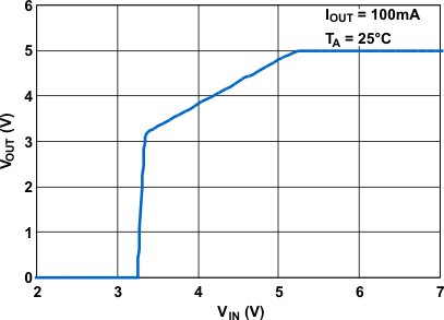
TPS7A63-Q1 TPS7A6401-Q1 g_vout_vin_lvsab1.gif
Figure 6. Output Voltage vs Input Voltage
(VOUT Set To 5 V)
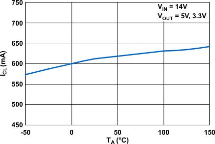
TPS7A63-Q1 TPS7A6401-Q1 g_icl_ta_lvsab1.gif
Figure 8. Output Current Limit vs Ambient Air Temperature
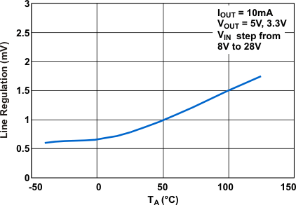
TPS7A63-Q1 TPS7A6401-Q1 g_linereg_ta_lvsab1.gif
Figure 10. Line Regulation vs Ambient Air Temperature
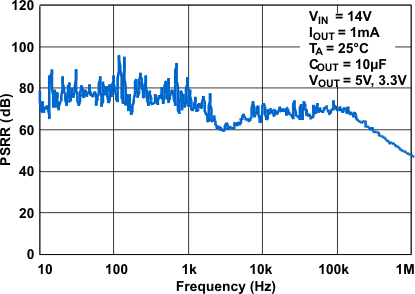
TPS7A63-Q1 TPS7A6401-Q1 g_psrr_light_lvsab1.gif
Figure 12. PSRR at Light Load Current