SLVSA98F May   2010  – March 2020 TPS7A65-Q1

PRODUCTION DATA.  

  1. Features
  2. Applications
  3. Description
    1.     Device Images
      1.      Typical Application Schematic
      2.      Typical Regulator Stability
  4. Revision History
  5. Pin Configuration and Functions
    1.     Pin Functions
  6. Specifications
    1. 6.1 Absolute Maximum Ratings
    2. 6.2 ESD Ratings
    3. 6.3 Recommended Operating Conditions
    4. 6.4 Thermal Information
    5. 6.5 Electrical Characteristics
    6. 6.6 Dissipation Ratings
    7. 6.7 Typical Characteristics
  7. Detailed Description
    1. 7.1 Overview
    2. 7.2 Functional Block Diagram
    3. 7.3 Feature Description
      1. 7.3.1 Power Up
      2. 7.3.2 Charge-Pump Operation
      3. 7.3.3 Low-Power Mode
      4. 7.3.4 Undervoltage Shutdown
      5. 7.3.5 Low-Voltage Tracking
      6. 7.3.6 Integrated Fault Protection
      7. 7.3.7 Thermal Shutdown
    4. 7.4 Device Functional Modes
      1. 7.4.1 Operation With VIN Lower Than 4 V
      2. 7.4.2 Operation With VIN Larger Than 4 V
  8. Application and Implementation
    1. 8.1 Application Information
    2. 8.2 Typical Application
      1. 8.2.1 Design Requirements
      2. 8.2.2 Detailed Design Procedure
      3. 8.2.3 Application Curve
  9. Power Supply Recommendations
  10. 10Layout
    1. 10.1 Layout Guidelines
      1. 10.1.1 Power Dissipation and Thermal Considerations
    2. 10.2 Layout Example
  11. 11Device and Documentation Support
    1. 11.1 Receiving Notification of Documentation Updates
    2. 11.2 Community Resources
    3. 11.3 Trademarks
    4. 11.4 Electrostatic Discharge Caution
    5. 11.5 Glossary
  12. 12Mechanical, Packaging, and Orderable Information

Package Options

Mechanical Data (Package|Pins)
Thermal pad, mechanical data (Package|Pins)
Orderable Information

Thermal Shutdown

This device incorporates a thermal shutdown (TSD) circuit as a protection from overheating. For continuous normal operation, the junction temperature should not exceed the TSD trip point. If the junction temperature exceeds the TSD trip point, the output turns off. When the junction temperature falls below the TSD trip point, the output turns on again. Figure 19 shows this.
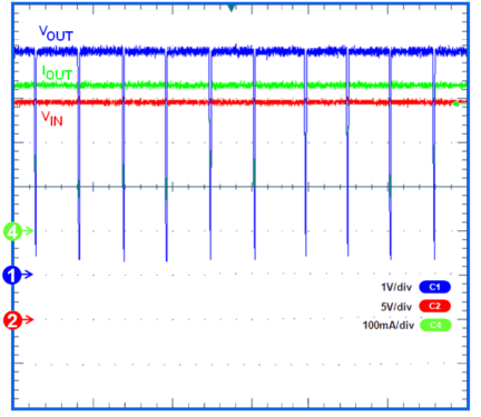
TPS7A65-Q1 thermal_cycling_waveform_lvsa98.gifFigure 19. Thermal Cycling Waveform for TPS7A6550-Q1 (VIN = 24 V, IOUT = 300 mA, VOUT = 5 V)