SLVSD64 December 2015 TPS7A6650H-Q1
PRODUCTION DATA.
- 1 Features
- 2 Applications
- 3 Description
- 4 Revision History
- 5 Pin Configuration and Functions
- 6 Specifications
- 7 Detailed Description
- 8 Application and Implementation
- 9 Power Supply Recommendations
- 10Layout
- 11Device and Documentation Support
- 12Mechanical, Packaging, and Orderable Information
Package Options
Mechanical Data (Package|Pins)
- DGN|8
Thermal pad, mechanical data (Package|Pins)
- DGN|8
Orderable Information
10 Layout
10.1 Layout Guidelines
10.1.1 Package Mounting
Solder pad footprint recommendations for the TPS7A6650H-Q1 are available at the end of this product data sheet and at www.ti.com.
10.1.2 Board Layout Recommendations to Improve PSRR and Noise Performance
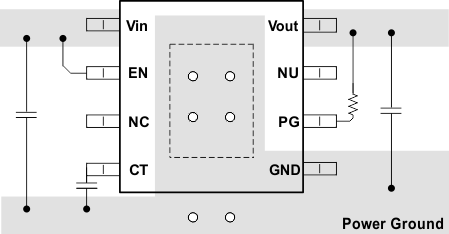
For the layout of TPS7A6650H-Q1, place the input and output capacitors close to the devices as shown in Figure 18. In order to enhance the thermal performance, TI recommends surrounding the device with some vias.
To improve ac performance such as PSRR, output noise, and transient response, TI recommends a board design with separate ground planes for Vin and Vout, with each ground plane connected only at the GND pin of the device. In addition, the ground connection for the output capacitor should connect directly to the GND pin of the device.
Minimize equivalent series inductance (ESL) and ESR in order to maximize performance and ensure stability. Place every capacitor as close as possible to the device and on the same side of the PCB as the regulator itself.
Do not place any of the capacitors on the opposite side of the PCB from where the regulator is installed. TI strongly discourages the use of vias and long traces because they may impact system performance negatively and even cause instability.
If possible, and to ensure the maximum performance specified in this product data sheet, use the same layout pattern used for the TPS7A6650H-Q1 evaluation board, available at www.ti.com.
10.2 Layout Example
 Figure 18. TPS7A6650H-Q1 Board Layout Diagram
10.3 Power Dissipation and Thermal Considerations
Calculate power dissipated in the device using Equation 2.
space

where:
PD = continuous power dissipation
IO = output current
V(Vin) = input voltage
V(Vout) = output voltage
As I(q) << IO, therefore ignore the term I(q) × V(Vin) in Equation 2.
For a device under operation at a given ambient air temperature (TA), calculate the junction temperature (TJ) using Equation 3.
space

where:
RθJA = junction-to-ambient air thermal impedance
space
