SBVS209D May 2013 – April 2017 TPS7A7002
PRODUCTION DATA.
- 1 Features
- 2 Applications
- 3 Description
- 4 Revision History
- 5 Pin Configuration and Functions
- 6 Specifications
- 7 Detailed Description
- 8 Application and Implementation
- 9 Power Supply Recommendations
- 10Layout
- 11Device and Documentation Support
- 12Mechanical, Packaging, and Orderable Information
Package Options
Mechanical Data (Package|Pins)
- DDA|8
Thermal pad, mechanical data (Package|Pins)
- DDA|8
Orderable Information
8 Application and Implementation
NOTE
Information in the following applications sections is not part of the TI component specification, and TI does not warrant its accuracy or completeness. TI’s customers are responsible for determining suitability of components for their purposes. Customers should validate and test their design implementation to confirm system functionality.
8.1 Application Information
The TPS7A7002 offers a high current supply with very-low dropout voltage, and it is designed to minimize the required component count for a simple, small-size, and low-cost solution. This section discusses the implementation of the TPS7A7002 LDO.
8.1.1 Input Capacitor (IN)
An input capacitor is not required for stability; however, TI recommends connecting a 1-µF to 10-µF low equivalent series resistance (ESR) capacitor across IN and GND as close as possible to the device.
8.1.2 Output Capacitor (OUT)
The TPS7A7002 is stable with standard ceramic capacitors with capacitance values from 4.7 μF to 47 μF without a feedforward capacitor. For output capacitors from 47 μF to 200 μF, a feedforward capacitor of at least 220 pF must be used. The TPS7A7002 is evaluated using an X5R-type, 10-μF ceramic capacitor. X5R- and X7R-type capacitors are recommended because of minimal variation in value and ESR over temperature. Maximum ESR must be less than 1 Ω.
As with any regulator, increasing the size of the output capacitor reduces overshoot and undershoot magnitude, but increases duration of the transient response.
8.1.3 Feedback Resistors (FB)
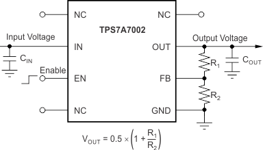
The voltage on the FB pin sets the output voltage and is determined by the values of R1 and R2. Use Equation 1 to calculate the values of R1 and R2 for any voltage.

Table 2 shows the recommended resistor values for the best performance of the TPS7A7002. If the values in Table 2 are not used, keep the value of R2 from 27 kΩ to 33 kΩ. In Table 2, E96 series resistors are used. For the actual design, pay attention to any resistor error factors.
Table 2. Sample Resistor Values for Common Output Voltages
| VOUT | R1 (kΩ) | R2 (kΩ) |
|---|---|---|
| 1 | 30.1 | 30.1 |
| 1.2 | 42.2 | 30.1 |
| 1.5 | 60.4 | 30.1 |
| 1.8 | 78.7 | 30.1 |
| 2.5 | 121 | 30.1 |
| 3 | 150 | 30.1 |
| 3.3 | 169 | 30.1 |
| 5 | 274 | 30.1 |
8.2 Typical Application
This section describes the implementation of the TPS7A7002, using the feedback pin to configure the output voltage and regulate a 2-A load at 1.4 V using a 1.6-V input voltage, operating in a temperature range of 25°C to 85°C. Figure 8 shows the schematic for this typical application circuit.
 Figure 8. Typical Application Schematic
8.2.1 Design Requirements
For this design example, use the parameters listed in Table 3 as the input parameters.
Table 3. Design Parameters
| PARAMETER | DESIGN REQUIREMENT |
|---|---|
| Input voltage | 1.6 V ±3% |
| Output voltage | 1.4 V ±3% |
| Maximum output current | 2 A |
| Ambient temperature | 25°C ≤ TA ≤ 75°C |
8.2.2 Detailed Design Procedure
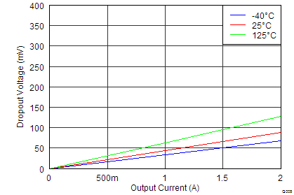
At IOUT = 2 A, the TPS7A7002 has a maximum dropout of less than 150 mV over temperature, as seen in Figure 9; thus, a 200-mV headroom is sufficient for operation over both input and output voltage accuracy.
To achieve 1.2 V on the output, choose the correct feedback resistors. The Feedback Resistors (FB) section suggests keeping the value of R2 in the range of 27 kΩ to 33 kΩ, so select R2 to be 30.1 kΩ, a standard resistor in the E96 series. Using Equation 1 to achieve a 1.4-V output, determine the size for R1 using Equation 2.
Given that R2 = 30.1 kΩ and VOUT = 1.4 V, R1 = 54.2 kΩ. The closest resistor in the E96 series is 53.6 kΩ, giving an output voltage within the output design requirements.
With a headroom voltage of 200 mV and a 2-A maximum load, the internal power dissipation is 400 mW, and corresponds to a 18.56°C junction temperature rise for the DDA package.
With a 75°C maximum ambient temperature as per design constraints, the junction temperature is at 93.56°C, and satisfies the recommended operating junction temperature range.
8.2.3 Application Curve

| VOUT = 1.4 V |