SBVS189G March 2012 – October 2023 TPS7A7100
PRODUCTION DATA
- 1
- 1 Features
- 2 Applications
- 3 Description
- 4 Pin Configurations
- 5 Specifications
- 6 Detailed Description
- 7 Application and Implementation
- 8 Device And Documentation Support
- 9 Revision History
- 10Mechanical, Packaging, And Orderable Information
Package Options
Refer to the PDF data sheet for device specific package drawings
Mechanical Data (Package|Pins)
- RGT|16
- RGW|20
Thermal pad, mechanical data (Package|Pins)
- RGT|16
Orderable Information
6.3.2 Traditional Adjustable Configuration
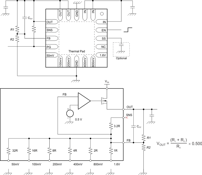
For any output voltage target that is not supported in the User-Configurable Output VoltageUser-Configurable Output Voltage section, a traditional adjustable configuration with external-feedback resistors can be used with the TPS7A7100. Figure 6-7 shows how to configure the TPS7A7100 as an adjustable regulator with an equation and Table 6-2 lists recommended pairs of feedback resistor values.
The bottom side of feedback resistor R2 in Figure 6-7 must be in the range of 27 kΩ to 33 kΩ to maintain the specified regulation accuracy.
 Figure 6-7 Traditional Adjustable Configuration With External Resistors
| VOUT(TARGET) (V) |
E96 SERIES | R40 SERIES | |||
|---|---|---|---|---|---|
| R1 (kΩ) | R2 (kΩ) | R1 (kΩ) | R2 (kΩ) | ||
| 1 | 30.1 | 30.1 | 30 | 30 | |
| 1.2 | 39.2 | 28 | 43.7 | 31.5 | |
| 1.5 | 61.9 | 30.9 | 60 | 30 | |
| 1.8 | 80.6 | 30.9 | 80 | 30.7 | |
| 1.9 | 86.6 | 30.9 | 87.5 | 31.5 | |
| 2.5 | 115 | 28.7 | 112 | 28 | |
| 3 | 147 | 29.4 | 150 | 30 | |
| 3.3 | 165 | 29.4 | 175 | 31.5 | |
| 5 | 280 | 30.9 | 243 | 27.2 | |