SBVS190F March 2012 – October 2023 TPS7A7300
PRODUCTION DATA
- 1
- 1 Features
- 2 Applications
- 3 Description
- 4 Pin Configurations
- 5 Specifications
- 6 Detailed Description
- 7 Application and Implementation
- 8 Device And Documentation Support
- 9 Revision History
- 10Mechanical, Packaging, And Orderable Information
Package Options
Refer to the PDF data sheet for device specific package drawings
Mechanical Data (Package|Pins)
- RGW|20
Thermal pad, mechanical data (Package|Pins)
Orderable Information
7.4.1.3 Estimating Junction Temperature
Using the thermal metrics ΨJT and ΨJB, as listed in the Thermal Information table, the junction temperature can be estimated with corresponding formulas (given in Equation 3). For backwards compatibility, an older θJC,Top parameter is listed as well.

where:
- PD is the power dissipation shown by Equation 2
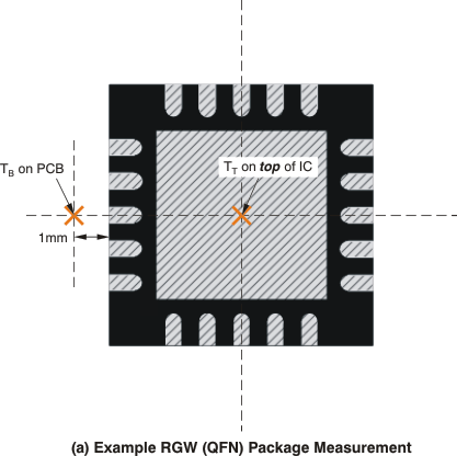
- TT is the temperature at the center-top of the device package
- TB is the PCB temperature measured 1 mm away from the device package on the PCB surface (see Figure 7-14)
Both TT and TB can be measured on actual application boards using a thermo-gun (an infrared thermometer).
For more information about measuring TT and TB, see the Using New Thermal Metrics application note.
 Figure 7-14 Measuring Points For
TT and TB
Figure 7-14 Measuring Points For
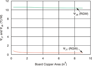
TT and TBFrom Figure 7-15, the new thermal metrics (ΨJT and ΨJB) are shown to have very little dependency on board size. That is, using ΨJT or ΨJB with Equation 3 is a good way to estimate TJ by simply measuring TT or TB, regardless of the application board size.
 Figure 7-15 ΨJT And ΨJB vs Board Size
For a more detailed discussion of why TI does not recommend using θJC(top) to determine thermal characteristics, see the Using New Thermal Metrics application note. For further information, see the Semiconductor and IC Package Thermal Metrics application note.