SBVS416B May   2022  – August 2022 TPS7A74

PRODUCTION DATA  

  1. Features
  2. Applications
  3. Description
  4. Revision History
  5. Pin Configuration and Functions
  6. Specifications
    1. 6.1 Absolute Maximum Ratings
    2. 6.2 ESD Ratings
    3. 6.3 Recommended Operating Conditions
    4. 6.4 Thermal Information
    5. 6.5 Electrical Characteristics
    6. 6.6 Typical Characteristics
  7. Detailed Description
    1. 7.1 Overview
    2. 7.2 Functional Block Diagram
    3. 7.3 Feature Description
      1. 7.3.1 Enable and Shutdown
      2. 7.3.2 Active Discharge
      3. 7.3.3 Global Undervoltage Lockout (UVLO) Circuit
      4. 7.3.4 Internal Current Limit
      5. 7.3.5 Thermal Shutdown Protection (TSD)
    4. 7.4 Device Functional Modes
      1. 7.4.1 Normal Operation
      2. 7.4.2 Dropout Operation
      3. 7.4.3 Disabled
    5. 7.5 Programming
      1. 7.5.1 Programmable Soft-Start
      2. 7.5.2 Sequencing Requirements
  8. Application and Implementation
    1. 8.1 Application Information
      1. 8.1.1 Adjusting the Output Voltage
      2. 8.1.2 Input, Output, and Bias Capacitor Requirements
      3. 8.1.3 Transient Response
      4. 8.1.4 Dropout Voltage
      5. 8.1.5 Output Noise
      6. 8.1.6 Estimating Junction Temperature
    2. 8.2 Typical Application
      1. 8.2.1 FPGA I/O Supply at 1.8 V With a Bias Rail
        1. 8.2.1.1 Design Requirements
        2. 8.2.1.2 Detailed Design Procedure
        3. 8.2.1.3 Application Curves
    3. 8.3 Power Supply Recommendations
    4. 8.4 Layout
      1. 8.4.1 Layout Guidelines
        1. 8.4.1.1 Estimating Junction Temperature
      2. 8.4.2 Layout Example
  9. Device and Documentation Support
    1. 9.1 Device Support
      1. 9.1.1 Development Support
        1. 9.1.1.1 Evaluation Modules
        2. 9.1.1.2 Spice Models
    2. 9.2 Documentation Support
      1. 9.2.1 Related Documentation
    3. 9.3 Receiving Notification of Documentation Updates
    4. 9.4 Support Resources
    5. 9.5 Trademarks
    6. 9.6 Electrostatic Discharge Caution
    7. 9.7 Glossary
  10. 10Mechanical, Packaging, and Orderable Information

Package Options

Mechanical Data (Package|Pins)
Thermal pad, mechanical data (Package|Pins)
Orderable Information

Application Curves

GUID-20220708-SS0I-GSZZ-C5RC-V8JTB1RWKK86-low.png
 CIN = COUT = 10 μF, CBIAS = 1 μF, VIN = 2.1 V, VBIAS = 6 V to 3.5 V to 6 V, IOUT = 1.5 A
Figure 8-3 VBIAS Line Transient
GUID-20220708-SS0I-3KZN-4R55-HQVMGZJGCN5B-low.png
CIN = COUT = 10 μF, CBIAS = 1 μF, VBIAS = 5 V, VIN = 2.1 V, IOUT = 10 mA to 1.5 A to 10 mA
Figure 8-5 Output Load Transient Response
GUID-20220708-SS0I-QPP9-J312-Q2TSQLZBW1MC-low.png
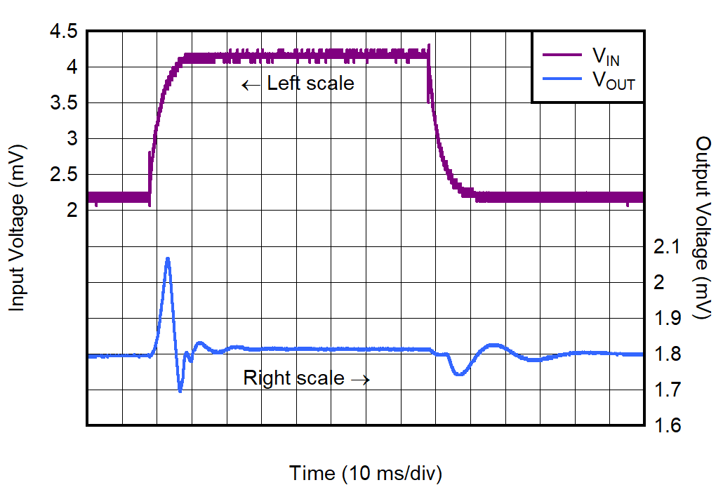
 CIN = COUT = 10 μF, CBIAS = 1 μF, VBIAS = 5 V, VIN = 2.1 V to 4.1 V to 2.1 V, IOUT = 1.5 A
Figure 8-4 VIN Line Transient
GUID-20220708-SS0I-PDWZ-5MNK-TH5SLC0QQM6P-low.png
CIN = COUT = 10 μF, CBIAS = 1 μF, VBIAS = 5 V, VIN = 2.1 V, IOUT = 0 mA
Figure 8-6 Turn-On Response