SBVS197F May 2013 – October 2015 TPS7A8300
PRODUCTION DATA.
- 1 Features
- 2 Applications
- 3 Description
- 4 Revision History
- 5 Pin Configurations and Functions
- 6 Specifications
-
7 Detailed Description
- 7.1 Overview
- 7.2 Functional Block Diagram
- 7.3
Feature Description
- 7.3.1 ANY-OUT Programmable Output Voltage
- 7.3.2 Adjustable Operation
- 7.3.3 ANY-OUT Operation
- 7.3.4 2-A LDO with an Internal Charge Pump
- 7.3.5 Low-Noise, 0.8-V Reference
- 7.3.6 Internal Protection Circuitry
- 7.3.7 Programmable Soft-Start
- 7.3.8 Power-Good Function
- 7.3.9 Integrated Resistance Network (ANY-OUT)
- 7.4 Device Functional Modes
- 8 Application and Implementation
- 9 Power-Supply Recommendations
- 10Layout
- 11Device and Documentation Support
- 12Mechanical, Packaging, and Orderable Information
Package Options
Mechanical Data (Package|Pins)
Thermal pad, mechanical data (Package|Pins)
Orderable Information
1 Features
- Ultralow Dropout: 125 mV Maximum at 2 A
- Output Voltage Noise: 6 µVRMS
- Power-Supply Ripple Rejection:
- 40 dB at 1 MHz
- Input Voltage Range:
- Without BIAS: 1.4 V to 6.5 V
- With BIAS: 1.1 V to 6.5 V
- Two Output Voltage Modes:
- 1.0% Accuracy Over Line, Load, and Temperature
- Stable with a 22-µF Output Ceramic Capacitor
- Programmable Soft-Start Output
- Power-Good (PG) Output
- Available Packages:
2 Applications
- RF, IF Components: VCO, ADC, DAC, LVDS
- Wireless Infrastructure: SerDes, FPGA, DSP™
- Test and Measurement
- Instrumentation, Medical, and Audio
3 Description
The TPS7A8300 is a low-noise (6 µVRMS), low-dropout voltage regulator (LDO) capable of sourcing a 2-A load with only 125 mV of maximum dropout.
The TPS7A8300 output voltages are fully user-adjustable (up to 3.95 V) using a printed circuit board (PCB) layout without the need of external resistors, thus reducing overall component count. For higher output voltage applications, the device achieves output voltages up to 5 V with the use of external resistors. The device supports very low input voltages (down to 1.1 V) with the use of an additional BIAS rail.
With very high accuracy (1% over line, load, and temperature), remote sensing, and soft-start capabilities to reduce inrush current, the TPS7A8300 is ideal for powering high-current, low-voltage devices such as high-end microprocessors and field-programmable gate arrays (FPGAs).
The TPS7A8300 is designed to power-up noise-sensitive components in high-speed communication applications. The very low-noise, 6-µVRMS device output and high broad-bandwidth PSRR (40 dB at
1 MHz) minimizes phase noise and clock jitter in high-frequency signals. These features maximize performance of clocking devices, analog-to-digital converters (ADCs), and digital-to-analog converters (DACs).
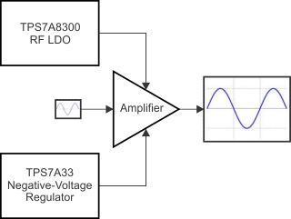
For applications where positive and negative low-noise rails are required, consider TI's TPS7A33 family of negative high-voltage, ultralow-noise linear regulators.
Device Information(1)
| PART NUMBER | PACKAGE | BODY SIZE (NOM) |
|---|---|---|
| TPS7A8300 | VQFN (20) | 5.00 mm × 5.00 mm |
| VQFN (20) | 3.50 mm × 3.50 mm |
- For all available packages, see the orderable addendum at the end of the datasheet.
4 Revision History
Changes from E Revision (August 2014) to F Revision
- Added title to page 1 graphic Go
- Updated ESD Ratings table to current standards Go
- Changed Figure 52: changed connection of EN pin Go
- Changed Enable (EN) and Undervoltage Lockout (UVLO) section: updated wording for better clarity on use of the Enable (EN) pin Go
Changes from D Revision (February 2013) to E Revision
- Changed format to meet latest data sheet standards; added new sections, and moved existing sectionsGo
- Changed first ANY-OUT sub-bullet of fifth Features bullet Go
- Changed eighth Features bullet: broke Soft-Start Output and PG Output into two separate Features bullets Go
- Changed first sentence of second paragraph in Description section Go
- Changed RGW and RGR drawings: removed spacing between number and unit in pins 5 to 7 and 9 to 11 Go
- Changed first row of Pin Functions table: deleted spacing between number and unit in pin namesGo
- Added capacitor value to BIAS pin description in Pin Functions tableGo
- Changed 87% to 89% in the PG pin description of the Pin Functions tableGo
- Changed thermal pad description in Pin Functions tableGo
- Changed conditions statements for Absolute Maximum Ratings and Recommended Operating Conditions tables Go
- Added Recommended Operating Conditions tableGo
- Changed the Typical Characteristics section: changed all curve titles and conditions Go
- Changed title of Figure 11 Go
- Added Overview section Go
- Changed second paragraph of Overview section: changed that can be groups, as follows to including Go
- Changed functional block diagram footnoteGo
- Added Feature Description sectionGo
- Changed adjustable version to adjustable configuration in first paragraph of Adjustable Operation section Go
- Changed Figure 51: removed right-hand side diagramGo
- Added Figure 52 Go
- Changed second sentence in Internal Charge Pump section Go
- Changed last sentence of UVLO sectionGo
- Changed oscillates to cycles in first paragraph of Thermal Protection sectionGo
- Changed first sentence of Programmable Soft-Start sectionGo
- Added Device Functional Modes sectionGo
- Added Application Information section Go
- Changed second paragraph of Noise sectionGo
- Added Typical Application section Go
- Added Figure 57 Go
Changes from C Revision (July 2013) to D Revision
- Changed document status from Mixed to Production DataGo
- Deleted footnote from second sub-bullet of last Features bulletGo
- Deleted footnote from RGR package drawingGo
- Changed GND pin description in Pin Descriptions tableGo
Changes from B Revision (July 2013) to C Revision
- Deleted PG Functionality sectionGo
- Changed Power-Good sectionGo
- Changed text in Feed-Forward Capacitor subsectionGo
Changes from A Revision (June 2013) to B Revision
- Changed from product preview to production data (mixed status)Go
Changes from * Revision (May 2013) to A Revision
- Changed product preview data sheetGo
