SBVS304B June 2017 – October 2021 TPS7A83A
PRODUCTION DATA
- 1 Features
- 2 Applications
- 3 Description
- 4 Revision History
- 5 Description (continued)
- 6 Pin Configuration and Functions
-
7 Specifications
- 7.1 Absolute Maximum Ratings
- 7.2 ESD Ratings
- 7.3 Recommended Operating Conditions
- 7.4 Thermal Information
- 7.5 Electrical Characteristics: General
- 7.6 Electrical Characteristics: TPS7A8300A
- 7.7 Electrical Characteristics: TPS7A8301A
- 7.8 Typical Characteristics: TPS7A8300A
- 7.9 Typical Characteristics: TPS7A8301A
- 8 Detailed Description
-
9 Application and Implementation
- 9.1
Application Information
- 9.1.1
External Component Selection
- 9.1.1.1 Adjustable Operation
- 9.1.1.2 ANY-OUT Programmable Output Voltage
- 9.1.1.3 ANY-OUT Operation
- 9.1.1.4 Increasing ANY-OUT Resolution for LILO Conditions
- 9.1.1.5 Recommended Capacitor Types
- 9.1.1.6 Input and Output Capacitor Requirements (CIN and COUT)
- 9.1.1.7 Feed-Forward Capacitor (CFF)
- 9.1.1.8 Noise-Reduction and Soft-Start Capacitor (CNR/SS)
- 9.1.2 Start Up
- 9.1.3 AC and Transient Performance
- 9.1.4 DC Performance
- 9.1.5 Sequencing Requirements
- 9.1.6 Negatively Biased Output
- 9.1.7 Reverse Current
- 9.1.8 Power Dissipation (PD)
- 9.1.1
External Component Selection
- 9.2 Typical Application
- 9.1
Application Information
- 10Power Supply Recommendations
- 11Layout
- 12Device and Documentation Support
- 13Mechanical, Packaging, and Orderable Information
Package Options
Mechanical Data (Package|Pins)
Thermal pad, mechanical data (Package|Pins)
Orderable Information
9.1.1.1 Adjustable Operation
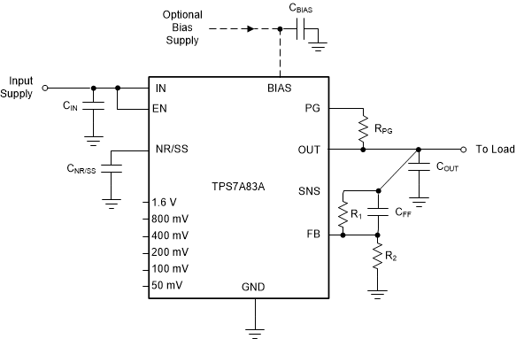
The TPS7A83A can be used either with the internal ANY-OUT network or by using external resistors. Using the ANY-OUT network allows the TPS7A83A to be programmed from 0.8 V to 3.95 V. For an output voltage range greater than 3.95 V and up to 5.2 V, external resistors must be used. This configuration is referred to as the adjustable configuration of the TPS7A83A throughout this document. Figure 9-1 shows that the output voltage is set by two resistors. 0.75% accuracy can be achieved with an external BIAS for VIN lower than 2.2 V.
 Figure 9-1 Adjustable Operation
Use Equation 1 to calculate R1 and R2 for any output voltage range. This resistive network must provide a current equal to or greater than 5 μA for dc accuracy. Use an R1 of approximately 12 kΩ to optimize the noise and PSRR.
Table 9-1 shows the resistor combinations required to achieve several common rails using standard 1%-tolerance resistors.
| NOMINAL OUTPUT VOLTAGE (V) |
FEEDBACK RESISTOR VALUES | CALCULATED OUTPUT VOLTAGE (V) |
|
|---|---|---|---|
| R1 (kΩ) | R2 (kΩ) | ||
| 0.90 | 12.4 | 100 | 0.899 |
| 0.95 | 12.4 | 66.5 | 0.949 |
| 1.00 | 12.4 | 49.9 | 0.999 |
| 1.10 | 12.4 | 33.2 | 1.099 |
| 1.20 | 12.4 | 24.9 | 1.198 |
| 1.50 | 12.4 | 14.3 | 1.494 |
| 1.80 | 12.4 | 10 | 1.798 |
| 1.90 | 12.1 | 8.87 | 1.890 |
| 2.50 | 12.4 | 5.9 | 2.480 |
| 2.85 | 12.1 | 4.75 | 2.838 |
| 3.00 | 12.1 | 4.42 | 2.990 |
| 3.30 | 11.8 | 3.74 | 3.324 |
| 3.60 | 12.1 | 3.48 | 3.582 |
| 4.50 | 11.8 | 2.55 | 4.502 |
| 5.00 | 12.4 | 2.37 | 4.985 |