SBVS291C April   2017  – December 2020 TPS7A84A

PRODUCTION DATA  

  1. Features
  2. Applications
  3. Description
  4. Revision History
  5. Pin Configuration and Functions
  6. Specifications
    1. 6.1 Absolute Maximum Ratings
    2. 6.2 ESD Ratings
    3. 6.3 Recommended Operating Conditions
    4. 6.4 Thermal Information
    5. 6.5 Electrical Characteristics: General
    6. 6.6 Electrical Characteristics: TPS7A8400A
    7. 6.7 Electrical Characteristics: TPS7A8401A
    8. 6.8 Typical Characteristics: TPS7A8400A
    9. 6.9 Typical Characteristics: TPS7A8401A
  7. Detailed Description
    1. 7.1 Overview
    2. 7.2 Functional Block Diagrams
    3. 7.3 Feature Description
      1. 7.3.1 Voltage Regulation Features
        1. 7.3.1.1 DC Regulation
        2. 7.3.1.2 AC and Transient Response
      2. 7.3.2 System Start-Up Features
        1. 7.3.2.1 Programmable Soft Start (NR/SS)
        2. 7.3.2.2 Internal Sequencing
          1. 7.3.2.2.1 Enable (EN)
          2. 7.3.2.2.2 Undervoltage Lockout (UVLO) Control
          3. 7.3.2.2.3 Active Discharge
        3. 7.3.2.3 Power-Good Output (PG)
      3. 7.3.3 Internal Protection Features
        1. 7.3.3.1 Foldback Current Limit (ICL)
        2. 7.3.3.2 Thermal Protection (Tsd)
    4. 7.4 Device Functional Modes
      1. 7.4.1 Regulation
      2. 7.4.2 Disabled
  8. Application and Implementation
    1. 8.1 Application Information
      1. 8.1.1 External Component Selection
        1. 8.1.1.1 Adjustable Operation
        2. 8.1.1.2 ANY-OUT Programmable Output Voltage
        3. 8.1.1.3 ANY-OUT Operation
        4. 8.1.1.4 Increasing ANY-OUT Resolution for LILO Conditions
        5. 8.1.1.5 Current Sharing
        6. 8.1.1.6 Recommended Capacitor Types
        7. 8.1.1.7 Input and Output Capacitor Requirements (CIN and COUT)
        8. 8.1.1.8 Feed-Forward Capacitor (CFF)
        9. 8.1.1.9 Noise-Reduction and Soft-Start Capacitor (CNR/SS)
      2. 8.1.2 Start-Up
        1. 8.1.2.1 Circuit Soft-Start Control (NR/SS)
          1. 8.1.2.1.1 Inrush Current
        2. 8.1.2.2 Undervoltage Lockout (UVLO)
        3. 8.1.2.3 Power-Good (PG) Function
      3. 8.1.3 AC and Transient Performance
        1. 8.1.3.1 Power-Supply Rejection Ratio (PSRR)
        2. 8.1.3.2 Output Voltage Noise
        3. 8.1.3.3 Optimizing Noise and PSRR
          1. 8.1.3.3.1 Charge Pump Noise
        4. 8.1.3.4 Load Transient Response
      4. 8.1.4 DC Performance
        1. 8.1.4.1 Output Voltage Accuracy (VOUT)
        2. 8.1.4.2 Dropout Voltage (VDO)
          1. 8.1.4.2.1 Behavior When Transitioning From Dropout Into Regulation
      5. 8.1.5 Sequencing Requirements
      6. 8.1.6 Negatively Biased Output
      7. 8.1.7 Reverse Current Protection
      8. 8.1.8 Power Dissipation (PD)
        1. 8.1.8.1 Estimating Junction Temperature
        2. 8.1.8.2 Recommended Area for Continuous Operation (RACO)
    2. 8.2 Typical Applications
      1. 8.2.1 Low-Input, Low-Output (LILO) Voltage Conditions
        1. 8.2.1.1 Design Requirements
        2. 8.2.1.2 Detailed Design Procedure
        3. 8.2.1.3 Application Curves
  9. Power Supply Recommendations
  10. 10Layout
    1. 10.1 Layout Guidelines
    2. 10.2 Layout Example
  11. 11Device and Documentation Support
    1. 11.1 Device Support
      1. 11.1.1 Development Support
        1. 11.1.1.1 Evaluation Models
        2. 11.1.1.2 Spice Models
    2. 11.2 Documentation Support
      1. 11.2.1 Related Documentation
    3. 11.3 Receiving Notification of Documentation Updates
    4. 11.4 Support Resources
    5. 11.5 Trademarks
    6. 11.6 Electrostatic Discharge Caution
    7. 11.7 Glossary

Package Options

Mechanical Data (Package|Pins)
Thermal pad, mechanical data (Package|Pins)
Orderable Information

Functional Block Diagrams

GUID-9896AED5-3B08-4D46-94BD-28C979804DC6-low.gif
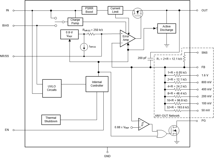
For the ANY-OUT network, the ratios between the values are highly accurate as a result of matching, but the actual resistance may vary significantly from the numbers listed.
Figure 7-1 TPS7A8400A Block Diagram
GUID-8CEA9CEB-1BE7-415D-8A3B-1ACBF239090D-low.gif
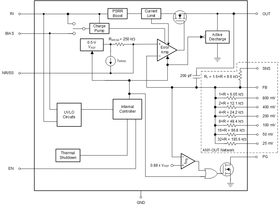
For the ANY-OUT network, the ratios between the values are highly accurate as a result of matching, but the actual resistance may vary significantly from the numbers listed.
Figure 7-2 TPS7A8401A Block Diagram