SBVS289A August 2017 – September 2017 TPS7A88-Q1
PRODUCTION DATA.
- 1 Features
- 2 Applications
- 3 Description
- 4 Revision History
- 5 Pin Configuration and Functions
- 6 Specifications
- 7 Detailed Description
- 8 Application and Implementation
- 9 Power Supply Recommendations
- 10Layout
- 11Device and Documentation Support
- 12Mechanical, Packaging, and Orderable Information
Package Options
Refer to the PDF data sheet for device specific package drawings
Mechanical Data (Package|Pins)
- RTJ|20
Thermal pad, mechanical data (Package|Pins)
Orderable Information
6 Specifications
6.1 Absolute Maximum Ratings
over operating junction temperature range and all voltages with respect to GND (unless otherwise noted)(1) (3)| MIN | MAX | UNIT | ||
|---|---|---|---|---|
| Voltage | INx, PGx, ENx | –0.3 | 7 | V |
| OUTx , SS_CTRLx | –0.3 | VINx + 0.3(2) | ||
| NR/SSx, FBx | –0.3 | 3.6 | ||
| Current | OUTx | Internally limited | Internally limited | A |
| PGx (sink current into device) | 5 | mA | ||
| Operating junction temperature, TJ | –55 | 150 | °C | |
| Storage temperature, Tstg | –55 | 150 | °C | |
(1) Stresses beyond those listed under Absolute Maximum Ratings may cause permanent damage to the device. These are stress ratings only, which do not imply functional operation of the device at these or any other conditions beyond those indicated under Recommended Operating Conditions. Exposure to absolute-maximum-rated conditions for extended periods may affect device reliability.
(2) The absolute maximum rating is VINx + 0.3 V or 7 V, whichever is smaller.
(3) Lowercase x indicates that the specification under consideration applies to both channel 1 and channel 2, one channel at a time.
6.2 ESD Ratings
| VALUE | UNIT | |||
|---|---|---|---|---|
| V(ESD) | Electrostatic discharge | Human-body model (HBM), per AEC Q100-002(1) | ±2000 | V |
| Charged-device model (CDM), per AEC Q100-011 | ±750 | |||
(1) AEC Q100-002 indicates that HBM stressing shall be in accordance with the ANSI/ESDA/JEDEC JS-001 specification.
6.3 Recommended Operating Conditions
over operating junction temperature range (unless otherwise noted)6.4 Thermal Information
| THERMAL METRIC(1) | TPS7A88-Q1 | UNIT | |
|---|---|---|---|
| RTJ (WQFN) | |||
| 20 PINS | |||
| RθJA | Junction-to-ambient thermal resistance | 39.8 | °C/W |
| RθJC(top) | Junction-to-case (top) thermal resistance | 27.7 | °C/W |
| RθJB | Junction-to-board thermal resistance | 16.9 | °C/W |
| ψJT | Junction-to-top characterization parameter | 0.3 | °C/W |
| ψJB | Junction-to-board characterization parameter | 16.6 | °C/W |
| RθJC(bot) | Junction-to-case (bottom) thermal resistance | 1.5 | °C/W |
(1) For more information about traditional and new thermal metrics, see theSemiconductor and IC Package Thermal Metrics application report.
6.5 Electrical Characteristics
over operating temperature range (TJ = –40°C to +140°C), VINx = 1.4 V, VOUTx(TARGET) = 0.8 V, IOUTx = 5 mA, VENx = 1.4 V, COUTx = 10 μF, CNR/SSx = 0 nF, CFFx = 0 nF, SS_CTRLx = GND, PGx pin pulled up to VINx with 100 kΩ, and for each channel; typical values are at TJ = 25°C (3) (unless otherwise noted)| PARAMETER | TEST CONDITIONS | MIN | TYP | MAX | UNIT | |
|---|---|---|---|---|---|---|
| VINx | Input supply voltage range | 1.4 | 6.5 | V | ||
| VREF | Reference voltage | 0.8 | V | |||
| VUVLO | Input supply UVLO | VINx rising | 1.31 | 1.39 | V | |
| VHYS | VUVLO Hysteresis | 290 | mV | |||
| VOUTx | Output voltage range | TJ = –40°C to +125°C | 0.8 – 1% | 5.15 + 1% | V | |
| 0.8 – 1.5% | 5.15 + 1% | |||||
| Output voltage accuracy(1)(2) | 0.8 V ≤ VOUTx ≤ 5.15 V 5 mA ≤ IOUTx ≤ 1 A TJ = –40°C to +125°C |
–1% | 1% | |||
| 0.8 V ≤ VOUTx ≤ 5.15 V 5 mA ≤ IOUTx ≤ 1 A |
–1.5% | 1% | ||||
| ΔVOUTx(ΔVINx) | Line regulation | IOUTx= 5 mA 1.4 V ≤ VINx ≤ 6.5 V |
0.003 | %/V | ||
| ΔVOUTx(ΔIOUTx) | Load regulation | 5 mA ≤ IOUTx ≤ 1 A | 0.03 | %/A | ||
| VDO | Dropout voltage | VINx ≥ 1.4 V 0.8 V ≤ VOUTx ≤ 5.15 V IOUTx = 1 A VFBx = 0.8 V – 3%, TJ = –40°C to +125°C |
225 | mV | ||
| VINx ≥ 1.4 V, 0.8 V ≤ VOUTx ≤ 5.15 V, IOUTx = 1 A, VFBx = 0.8 V – 3% |
250 | mV | ||||
| ILIM | Output current limit | VOUTx forced at 0.9 × VOUTx(TARGET), VINx = VOUTx(TARGET) + 300 mV |
1.5 | 1.7 | 1.9 | A |
| IGND | GND pin current | Both channels enabled, per channel VINx = 6.5 V, IOUTx = 5 mA |
2.1 | 3.5 | mA | |
| Both channels enabled, per channel VINx = 1.4 V, IOUTx = 1 A |
4 | |||||
| ISDN | Shutdown GND pin current | Both channels shutdown, per channel, PGx = (open) VINx = 6.5 V VENx = 0.4 V |
0.1 | 15 | μA | |
| IENx | ENx pin current | VINx = 6.5 V 0 V ≤ VENx ≤ 6.5 V |
–0.5 | 0.5 | μA | |
| VIL(ENx) | ENx pin low-level input voltage (device disabled) | 0 | 0.4 | V | ||
| VIH(ENx) | ENx pin high-level input voltage (device enabled) | 1.1 | 6.5 | V | ||
| ISS_CTRLx | SS_CTRLx pin current | VINx = 6.5 V 0 V ≤ VSS_CTRLx ≤ 6.5 V |
–0.2 | 0.2 | μA | |
| VIT(PGx) | PGx pin threshold | For PGx transitioning low with falling VOUTx; expressed as a percentage of VOUTx(TARGET) | 82% | 88.9% | 93% | |
| Vhys(PGx) | PGx pin hysteresis | For PGx transitioning high with rising VOUTx; expressed as a percentage of VOUTx(TARGET) | 1% | |||
| VOL(PGx) | PGx pin low-level output voltage | VOUTx < VIT(PGx), IPGx = –1 mA (current into device) | 0.4 | V | ||
| Ilkg(PGx) | PGx pin leakage current | VOUTx > VIT(PGx)
VPGx = 6.5 V |
1 | µA | ||
| INR/SSx | NR/SSx pin charging current | VNR/SSx = GND 1.4 V ≤ VINx ≤ 6.5 V VSS_CTRLx = GND |
4 | 6.2 | 10 | µA |
| VNR/SSx = GND 1.4 V ≤ VINx ≤ 6.5 V VSS_CTRLx = VINx |
65 | 100 | 150 | |||
| IFBx | FBx pin leakage current | VINx = 6.5 V VFBx = 0.8 V |
–100 | 100 | nA | |
| PSRR | Power-supply ripple rejection | f = 500 kHz VINx = 3.8 V VOUTx = 3.3 V IOUTx = 750 mA CNR/SSx = 10 nF CFFx = 10 nF |
40 | dB | ||
| Vn | Output noise voltage | BW = 10 Hz to 100 kHz VINx = 1.8 V VOUTx = 0.8 V IOUTx = 1 A CNR/SSx = 1 µF CFFx = 100 nF |
3.8 | μVRMS | ||
| Noise spectral density | f = 10 kHz VINx = 1.8 V VOUTx = 0.8 V IOUTx = 1 A CNR/SSx = 10 nF CFFx = 10 nF |
11 | nV/√Hz | |||
| Rdiss | Output active discharge resistance | VENx = GND | 250 | Ω | ||
| Tsd | Thermal shutdown temperature | Shutdown, temperature increasing | 160 | °C | ||
| Reset, temperature decreasing | 140 | |||||
(1) When the device is connected to external feedback resistors at the FBx pin, external resistor tolerances are not included.
(2) The device is not tested under conditions where VINx > VOUTx + 2.5 V and IOUTx = 1 A; the power dissipation is higher than the maximum rating of the package. This accuracy specification does not apply on any application condition that exceeds the power dissipation limit of the package under test.
(3) Lowercase x indicates that the specification under consideration applies to both channel 1 and channel 2, one channel at a time.
6.6 Typical Characteristics
at TJ = 25°C, 1.4 V ≤ VINx < 6.5 V, VINx ≥ VOUTx(TARGET) + 0.3 V, VOUTx = 0.8 V, SS_CTRLx = GND, IOUTx = 5 mA, VENx = 1.1 V, COUTx = 10 μF, CNR/SSx = 0 nF, CFFx = 0 nF, PGx pin pulled up to VOUTx with 100 kΩ, and SS_CTRLx = GND (unless otherwise noted)
| VOUTx = 1.2 V, VINx = VENx = 1.7 V COUTx = 10 µF CNR/SSx = CFFx = 10 nF |

| VOUTx = 1.2 V, IOUTx = 1.0 A, COUTx = 10 µF, CNR/SSx = CFFx = 10 nF |

| VOUTx = 1.2 V, VINx = VENx = 1.7 V, IOUTx = 1 A, CFFx = 10 nF |

| VOUTx = 1.8 V, IOUTx = 100 mA, COUTx = 10 µF, CNR/SSx = CFFx = 10 nF |

| VINx = 1.7 V, VOUTx = 1.2 V, IOUTx = 1A, VRMS BW = 10 Hz to 100 kHz, COUTx = 10 µF, CFFx = 10 nF |

| VOUTx = 1.2 V, IOUTx = 1 A, COUTx = 10 µF, CNR/SSx = 10 nF | ||
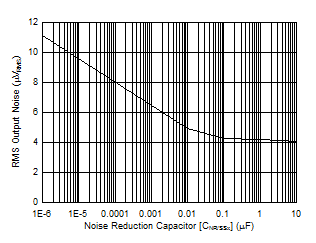
| VOUTx = 1.8 V, IOUTx = 1 A, CFFx = 0.01 µF, BW = 10 Hz to 100 kHz |
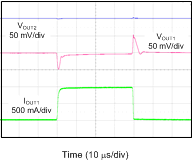
| VINx = 1.5 V, VOUTx = 1.2 V, IOUTx = 100 mA to 1 A to 100 mA at 1 A/µs, COUTx = 10 µF |
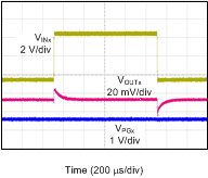
| VINx = 1.4 V to 6.5 V to 1.4 V at 2 V/µs, VOUTx = 0.8 V, IOUTx = 1 A, CNR/SSx = CFFx = 10 nF |

| VINx = 1.4 V, SS_CTRLx = GND, CNR/SSx = 10 nF |

| VINx = 1.4 V, SS_CTRLx = VINx, CNR/SSx = 1 µF |

| IOUTx = 1 A. VFB = 95% × VFB(nom) |

| VINx = 1.4 V, VOUTx = 0.8 V |

| VINx = 3.6 V, VOUTx = 3.3 V |

| VINx = 5.3 V, VOUTx = 5 V |

| Both channels enabled |

| VINx = 1.4 V, 6.5 V |

| VINx = VPGx = 6.5 V |

| SS_CTRLx = VINx |

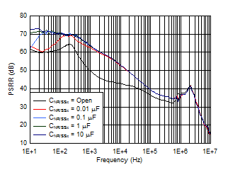
| VOUTx = 1.2 V, VINx = VENx = 1.7 V, IOUTx = 1 A, COUTx = 10 µF, CFFx = 10 nF |

| VOUTx = 3.3 V, VINx = VENx = 3.8 V, COUTx = 10 µF, CNR/SSx = CFFx = 10 nF |
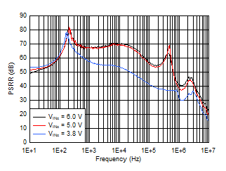
| VOUTx = 3.3 V, IOUTx = 1 A, COUTx = 10 µF, CNR/SSx = CFFx = 10 nF |

| VINx = VOUTx + 1 V, IOUTx = 1 A, VRMS BW = 10 Hz to 100 kHz, COUTx = 10 µF, CNR/SSx = CFFx = 10 nF |

| VINx = 3.8 V, VOUTx = 3.3 V, IOUTx = 1 A, VRMS BW = 10 Hz to 100 kHz, COUTx = 10 µF, CNR/SSx = 10 nF |

| VOUTx = 1.8 V, IOUTx = 1 A, VRMS BW = 10 Hz to 100 kHz, CFFx = 0.01 µF |

| VOUTx = 1.8 V, IOUTx = 1 A, CNR/SSx = 1 µF, BW = 10 Hz to 100 kHz |

| VINx = 5.5 V, VOUTx = 5.0 V, IOUTx = 100 mA to 1 A to 100 mA at 1 A/µs, COUTx = 10 µF |

| VINx = 1.4 V, SS_CTRLx = GND, CNR/SSx = 0 nF | ||

| VINx = 1.4 V, SS_CTRLx = VINx, CNR/SSx = 10 nF |

| VINx = 5.5 V. VFB = 95% × VFB(nom) |

| Both channels |

| VOUTx = 0.8 V, IOUTx = 50 mA |

| VOUTx = 3.3 V, IOUTx = 10 mA |

| VOUTx = 5 V, IOUTx = 5 mA |

| Both channels enabled |

| VINx = 1.4 V, 6.5 V |

| SS_CTRLx = GND |

| VINx = 1.4 V |

| VINx = 1.4 V |