SBVS336C september 2021 – june 2023 TPS7A94
PRODUCTION DATA
- 1
- 1 Features
- 2 Applications
- 3 Description
- 4 Revision History
- 5 Pin Configuration and Functions
- 6 Specifications
-
7 Detailed Description
- 7.1 Overview
- 7.2 Functional Block Diagram
- 7.3
Feature Description
- 7.3.1 Output Voltage Setting and Regulation
- 7.3.2 Ultra-Low Noise and Ultra-High Power-Supply Rejection Ratio (PSRR)
- 7.3.3 Programmable Current Limit and Power-Good Threshold
- 7.3.4 Programmable Soft Start (NR/SS Pin)
- 7.3.5 Precision Enable and UVLO
- 7.3.6 Active Discharge
- 7.3.7 Thermal Shutdown Protection (TSD)
- 7.4 Device Functional Modes
-
8 Application and Implementation
- 8.1
Application Information
- 8.1.1 Output Voltage Restart (Overshoot Prevention Circuit)
- 8.1.2 Precision Enable (External UVLO)
- 8.1.3 Undervoltage Lockout (UVLO) Operation
- 8.1.4 Dropout Voltage (VDO)
- 8.1.5 Power-Good Feedback (FB_PG Pin) and Power-Good Threshold (PG Pin)
- 8.1.6 Adjusting the Factory-Programmed Current Limit
- 8.1.7 Programmable Soft-Start and Noise-Reduction (NR/SS Pin)
- 8.1.8 Inrush Current
- 8.1.9 Optimizing Noise and PSRR
- 8.1.10 Adjustable Operation
- 8.1.11 Paralleling for Higher Output Current and Lower Noise
- 8.1.12 Recommended Capacitor Types
- 8.1.13 Load Transient Response
- 8.1.14 Power Dissipation (PD)
- 8.1.15 Estimating Junction Temperature
- 8.1.16 TPS7A94EVM-046 Thermal Analysis
- 8.2 Typical Application
- 8.3 Power Supply Recommendations
- 8.4 Layout
- 8.1
Application Information
- 9 Device and Documentation Support
- 10Mechanical, Packaging, and Orderable Information
Package Options
Refer to the PDF data sheet for device specific package drawings
Mechanical Data (Package|Pins)
- DSC|10
Thermal pad, mechanical data (Package|Pins)
Orderable Information
7.3.1 Output Voltage Setting and Regulation
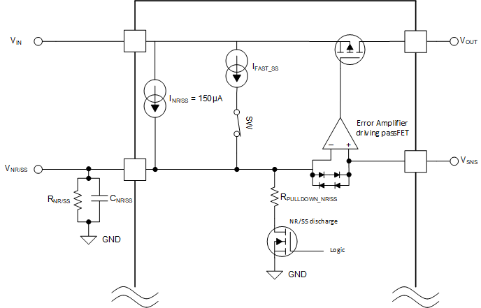
Figure 7-1 shows a simplified regulation circuit, where the input signal (VNR/SS) is generated by the internal current source (INR/SS) and the external resistor (RNR/SS). Because the error amplifier is always operating in unity-gain configuration, the LDO output voltage is directly programmed by the VNR/SS voltage. The VNR/SS reference voltage is generated by an internal low-noise current source driving the RNR/SS resistor and is designed to have very low bandwidth at the input to the error amplifier through the use of a low-pass filter (CNR/SS || RNR/SS).

This unity-gain configuration, along with the highly accurate INR/SS reference current, enables the device to achieve excellent output voltage accuracy; though, the RNR/SS accuracy can become the limiting factor when operating at low output voltage. The low dropout voltage (VDO) enables reduced thermal dissipation and achieves robust performance. This combination of features makes this device an excellent voltage source for powering sensitive analog low-voltage devices.