SBVS415A april 2023 – july 2023 TPS7A96
PRODUCTION DATA
- 1
- 1 Features
- 2 Applications
- 3 Description
- 4 Revision History
- 5 Pin Configuration and Functions
- 6 Specifications
-
7 Detailed Description
- 7.1 Overview
- 7.2 Functional Block Diagram
- 7.3
Feature Description
- 7.3.1 Output Voltage Setting and Regulation
- 7.3.2 Ultra-Low Noise and Ultra-High Power-Supply Rejection Ratio (PSRR)
- 7.3.3 Programmable Current Limit and Power-Good Threshold
- 7.3.4 Programmable Soft-Start (NR/SS Pin)
- 7.3.5 Precision Enable and UVLOs
- 7.3.6 Active Discharge
- 7.3.7 Thermal Shutdown Protection (TSD)
- 7.4 Device Functional Modes
-
8 Application and Implementation
- 8.1
Application Information
- 8.1.1 Output Voltage Restart (Overshoot Prevention Circuit)
- 8.1.2 Precision Enable (External UVLO)
- 8.1.3 Undervoltage Lockout (UVLO) Operation
- 8.1.4 Dropout Voltage (VDO)
- 8.1.5 Power-Good Feedback (FB_PG Pin) and Power-Good Threshold (PG Pin)
- 8.1.6 Adjusting the Factory-Programmed Current Limit
- 8.1.7 Programmable Soft-Start and Noise-Reduction (NR/SS Pin)
- 8.1.8 Inrush Current
- 8.1.9 Optimizing Noise and PSRR
- 8.1.10 Adjustable Operation
- 8.1.11 Paralleling for Higher Output Current and Lower Noise
- 8.1.12 Recommended Capacitor Types
- 8.1.13 Load Transient Response
- 8.1.14 Power Dissipation (PD)
- 8.1.15 Estimating Junction Temperature
- 8.1.16 TPS7A96EVM-106 Thermal Analysis
- 8.2 Typical Application
- 8.3 Power Supply Recommendations
- 8.4 Layout
- 8.1
Application Information
- 9 Device and Documentation Support
- 10Mechanical, Packaging, and Orderable Information
Package Options
Mechanical Data (Package|Pins)
- DSC|10
Thermal pad, mechanical data (Package|Pins)
- DSC|10
Orderable Information
3 Description
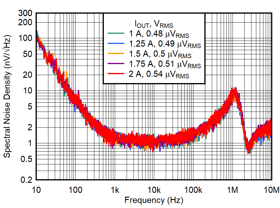
The TPS7A96 is an ultra-low noise (0.5 μVRMS), low-dropout (LDO) voltage regulator capable of sourcing 2 A with only 200 mV of dropout. The low dropout, in conjunction with a wide bandwidth error amplifier, allows for very high PSRR (104 dB at 1 kHz and 48 dB at 1 MHz) under low operating headroom (500 mV) and high output current (1.75 A).
The device output is adjustable from 0.4 V to 5.5 V with an external resistor. With the wide input voltage range, the device supports operation as low as 1.9 V and up to 5.7 V. The device includes a programmable current limit, programmable PG threshold, and precision enable, allowing better control in the application.
With the high-accuracy reference and wide-bandwidth topology, the device can be easily paralleled to achieve lower noise and higher current.
With 1% output voltage accuracy (over line, load, and temperature) and soft-start capabilities to reduce inrush current, the device is designed for powering sensitive analog low-voltage devices.
 Ultra-Low Output Noise Independent of Output
Voltage (10 Hz–100 kHz)
 Typical Application Circuit